Remote Flying Fish Project Part 8: PCB Design (PCB Layout)
Follow article Dave from DesignSpark
How do you feel about this article? Help us to provide better content for you.
Dave from DesignSpark
Thank you! Your feedback has been received.
Dave from DesignSpark
There was a problem submitting your feedback, please try again later.
Dave from DesignSpark
What do you think of this article?
Had having fun with the schematic part and now moved on to PCB layout? Let's begin.
Followed by the PCB translation button being clicked, there are still options to be configured before you can get the .pcb file of a 2-layer board generated.
The website below tells you how to do it. Start reading How can I convert schematics to PCB? in Zendesk and also take reference of the aforementioned YouTube video series part 6:
P.S: For the unit settings, I chose mm for all of them.
After that, you should be seeing something like this
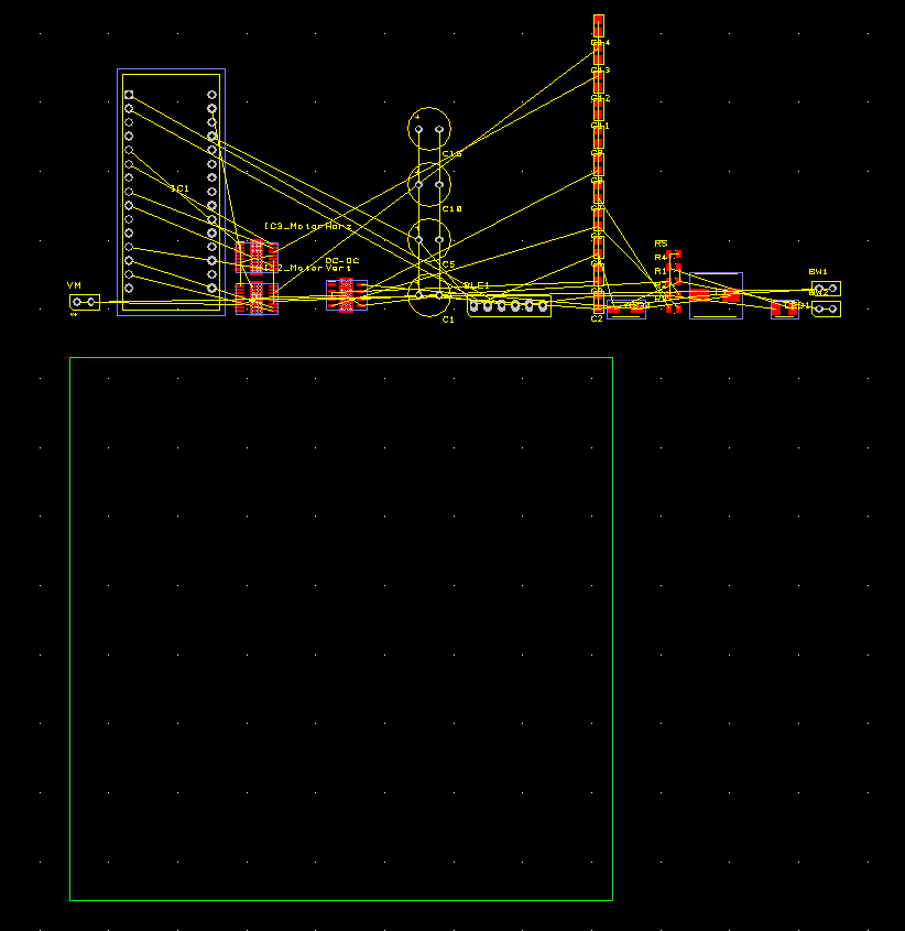
And there are a total of 3 pieces in my design:
- mainboard - all ICs components to place onto
- side propeller stripe - to hold the side motors
- connector stripe - connect the fish ball and PCB
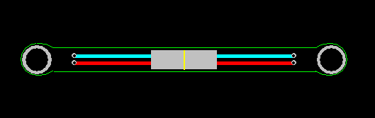
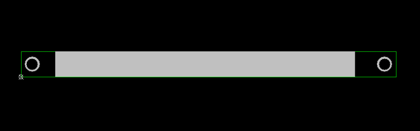
The side propeller stripe and the connector are not separated into two because of the extra charge of the manufacturer. We can simply cut them by using pilers.
As a result, a list of tasks is required for you to complete.
[!!! IMPORTANT !!! ]
After completing the list of tasks, simply output the Gerber files and send them to the PCB fabrication merchants over the Internet.
Hence, you will need to first figure out which PCB manufacturer to order from, and then obtain the important information from them. For example: min drilling aperture, min pad diameter, min track width, min track spacing, etc.
These parameters are going to affect your design seriously if you missed them by accident.
The task list:
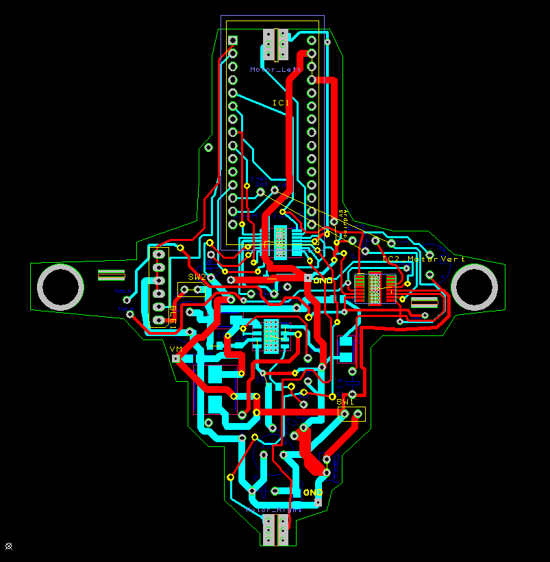
1. Place all components into the outlined(green box) area.
2. Set up the track width of each of the net classes/ individual nets, you could make use of the calculator here: https://www.7pcb.com/trace-width-calculator.php
Note: Please be reminded that the pin width limits the track width
3.Also setup the min separation gap between tracks, vias, and pads.
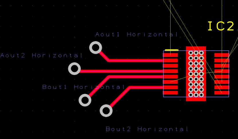
4. Add tracks to eliminate all the air wires(the yellow lines).
ALSO, remember to draw an extension line and add pads of the Aout and Bout pins in use of the DRV8833 motor drivers. Otherwise, you will be making a piece of defective PCB.
5. Fine-tune the position, reposition the components, if necessary, to reduce space occupied.
6. Use Design Rule Check(DRC) to see if the connections are all correct and the design has no-fault. (I am not using it because I was not familiarized enough, so I just do the checking on my bare eyes, lol.. which turned out I had mistaken RST and 5V pin of Arduino, and I will talk about it in later part)
Question: There isn't really a place you can observe from the PCB layout is reserved for Battery, why? (Ans in next chapter)
As you completed all tasks, you are recommended to follow How do I produce Gerber files? to proceed Gerber file generation, or YouTube video series part 7: https://www.youtube.com/watch?v=kwpS0pb4vLU&list=PLv91f6GOku19l_WuhdYn6SaaX19zEX-V9
In addition, I would like to briefly introduce the default layers and mechanical layers.
After pressing Shift+P, go to the "layer" tab and you should the screen below that lists out all the layers involved in the current PCB design.
- Board Outline: tells the shape of the board
- Top Documentation: marking only display in document, not PCB
- Top Silkscreen: marking display in both document and PCB
- Top Copper: marked area for soldering (connect the board + components)
- Bottom xxxxx: same functionality but just the other side of the board
Then you may also wonder if you can add some cuttings inside the PCB area. And the answer is definitely yes. In DS PCB, the mechanical layer is the corresponding layer indicating the cutting. However, such a layer does not exist by default.
Step to add:
- press Shift+T to open Design Technology
- click "Add"
- setup as shown below
- The arrow pointed row is the result after adding.
- Apply
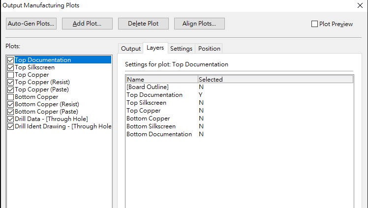
- press Shift+P to open Output Manufacturing Plots
- click "Add Plot"
- Setup as follow
- Done
- Remark: to use mechanical layer, user "Add shape" instead of "Add board", as you are only allowed to change the layer of shape


And, not much to say, but just that PCB design is a long process when you first get into touch with it.
PLEASE, BE PATIENT ENOUGH TO AVOID MISTAKES.
ALSO, TRIAL AND ERROR WILL LEAD YOU TO SUCCESS
Last but not least, here are some tips for you to facilitate the PCB positioning and routing procedure.
- setup the Grid size in setting
- setup the system origin to the bottom left corner of the default outline, so it represents (0,0)
- use Shift+Click to select all connected elements (e.g. whole square instead of one side of the square)
- use F to flip(mirror) element
- use Q to change the side of the track (top to bottom/ bottom to top)
- use R to rotate the element
- after selecting an element(s), use Alt+Enter to open the property windows
- use Shift+= to fine-tune the position of an element
- use = to set the exact coordinates of an element
- double click a track or use Click -> Shift+A to make an extra joint of a track
- Point 7 also applies to the board outline


In the next chapter, we will move forward to do soldering.
Parts in this series
- Remote Flying Fish Project Part 1: Introduction
- Remote Flying Fish Project Part 2: DIY Series - Arduino Testing
- Remote Flying Fish Project Part 3: Motor Testing
- Remote Flying Fish Project Part 4: Bluetooth Testing
- Remote Flying Fish Project Part 5: Motor Testing with Remote XY
- Remote Flying Fish Project Part 6: PCB Design (preparatory)
- Remote Flying Fish Project Part 7: PCB Design (Schematic)
- Remote Flying Fish Project Part 8: PCB Design (PCB Layout)
- Remote Flying Fish Project Part 9: Soldering and Arduino Programming
- Remote Flying Fish Project Part 10: Flutter Introduction
- Remote Flying Fish Project Part 11: Flutter Installation on MacOS
- Remote Flying Fish Project Part 12: Flutter Installation on Windows
Comments