
- Navigate the DesignSpark PCB drawing software interface confidently
Learn DesignSpark PCB
Learn PCB design and drawing — from schematic to manufacturing-ready output — with our step-by-step DesignSpark PCB tutorials. Whether you're designing your first board or refining an advanced workflow, our guides cover everything from navigating the interface and placing components to running DRC checks and generating Gerber files.
After Completing these Tutorials, You Will be Able to:
- Create a schematic from scratch and translate it to a PCB layout
- Place and manage components using 2D models and libraries
- Run Design Rules Checks (DRC) to catch errors before manufacture
DesignSpark PCB Software Tutorials
Get step-by-step DesignSpark PCB tutorials for beginner, intermediate and advanced engineers. Our tutorials cover the full design workflow, from navigating the interface and capturing schematics to working with component libraries and generating manufacturing-ready Gerber outputs.
Getting started
Find out how to Download, install, and get logged into the software
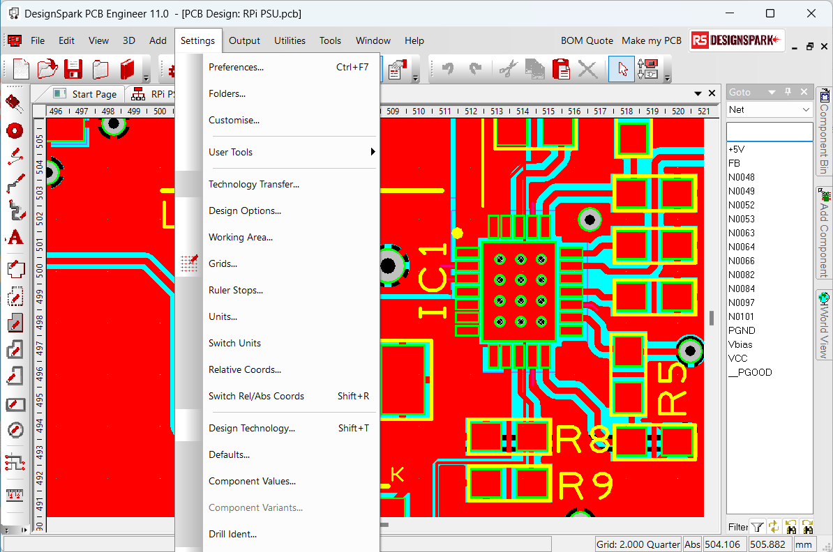
The PCB User Interface
Learn how to naviagate and use the functions within the software
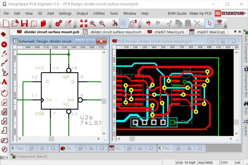
Starting a New PCB Project
Learn how to create and build your first PCB Design from Schematic to PCB Layout

Working with Components
Understanding and working with 2D models and libraries
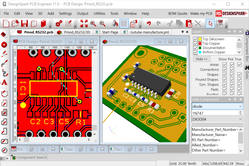
Creating your PCB Design
Find out how to use features within the software to complete your project design
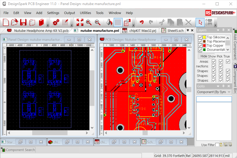
Preparing your PCB for Manufacture
Preparing your PCB design Project ready for manufacture
DesignSpark PCB Version 12: New Feature Tutorials
Explore the latest additions to DesignSpark PCB Version 12. These short tutorials walk through each new feature so you can get up to speed quickly and make the most of your updated software
How do I use the component bin sort and filter options?
How do I use dual units and angular precision in the Measure tool?
How do I translate to PCB based on an existing design?
How do pre-plot checks help me with correct layer selection?
How do I save the library of parts from my project?
How do I save an independent copy of my DSPCB file?
How do I sequentially number multiple named pins in my schematic?
How do I export a custom library component for sharing or backup?

Download DesignSpark PCB Design Software
Start designing with the DesignSpark Explorer plan — free for personal and commercial use, with unlimited layers, schematic sheets and manufacturing outputs. No hidden fees, no time limits.

Effortless Multi-License Setup for Your Team
A multi-seat licence gives engineering managers flexibility and control.
- Manage your team and reassign licences as your team evolves
- Improve collaboration, your whole team can now access 3 professional CAD tools
- Count savings because the more seats, the bigger the discount.
Join the DesignSpark PCB Community
You might find it helpful to use our other resources to support your learning. We have a dedicated forum and plenty of articles to browse through. Find inspiration, receive support and share your work with other DesignSpark PCB creators.
If you need more assistance, you can visit our PCB Software FAQs page
Bonjour,
J'essaie d'installer DesignSpark PCB 13.0.3 sur Windows 11, mais le logiciel refuse de démarrer.
Le message d'erreur indique :
« Init.dll n'est pas conçu pour s'exécuter sous Windows ou il contient une erreur. État de l'erreur : 0xc0e90002. »
Après vérification dans l'Observateur d'événements Windows, j'ai constaté un événement CodeIntegrity 3077 indiquant que "DesignSpark.exe" tente de charger "Init.dll", mais que le fichier ne respecte pas les exigences de signature de la stratégie de sécurité.
Le fichier "Init.dll" affiche la version 29.0.4.2 et ne présente aucune signature numérique dans ses propriétés. Smart App Control est activé sur mon PC.
J'ai déjà réinstallé le logiciel à partir de l'installateur officiel "DesignSparkPCB_V13_0_3", dont la version du fichier est 13.0.3002.0, sans résoudre le problème.
Pourriez-vous m'indiquer comment faire fonctionner cette version sous Windows 11 avec Smart App Control activé, ou me fournir un correctif officiel ?
Merci pour votre aide. Hi everyone,
I'm a beginner in PCB design, and honestly, I'm finding it a bit harder than I expected!
I'm trying to understand things like component placement, routing traces, choosing the right number of layers, and making sure the board will actually work when manufactured. There seem to be so many things to consider, and I'm not always sure what I should focus on first.
I'd love to hear about your own experiences, especially anything you wish you'd known when you first started designing PCBs.
Thanks in advance for any advice! When designing a PCB, we usually focus on component placement, routing, trace width, clearances, and signal integrity. But what about solder mask color? Does it make any practical difference in inspection, assembly, or long-term maintenance, or is it mainly an aesthetic choice?
Green is still a common choice for production boards, but black, blue, red, and white solder masks are also widely seen in different applications. For example, black can give a product a clean appearance, while white can be useful for LED boards because of its reflective surface. On the other hand, darker solder masks may make some solder joints or defects harder to spot during visual inspection.
I was looking into the practical differences between these options and came across some discussions of PCB manufacturing requirements, including the color options offered by manufacturers such as PCBCool.
I'm curious about what other engineers have experienced in actual projects.
Have you noticed any meaningful difference in visual inspection when working with different solder mask colors?
Do you consider solder mask color during the initial PCB design stage, or decide it later based on the product enclosure and appearance?
Have you encountered any manufacturing, cost, or lead-time differences when choosing a non-standard color?
I'd be interested to hear your experiences, particularly from people who have designed and manufactured boards in production quantities. Are there situations where you'd strongly recommend one color over another? I have encountered a Catch 22 situation a number of times.
Here is a simple example that illustrates the problem:-
Create a schematic with two resistors and connect them together with a single net: N0001
Translate the schematic to a PCB.
Rename the Net on the PCB from N0001 to N0002
Rename the Net on the Schematic from N0001 to N0003
Now try and forward the design change to the PCB.
If you try to run Back Annotation as suggested it fails with the following error:-
===
Back Annotate renames from the PCB design to all Schematic designs in project "Test1".
Error: Could not find Net " N0001".
===
You are now completely stuck.
If you manually change N0002 on the PCB to match the Schematic (i.e. N0003) this is what happens:-.
However if you now try to forward design changes from the Schematic you get this:-
Attempting Back annotation again gives another error:-
===
Back Annotate renames from the PCB design to all Schematic designs in project "Test1".
Error: Could not find Net " N0001".Error: Could not find Net " N0002".
===
For those old enough to remember the Colossal Cave adventure program: "You are in a maze of twisty passageways , all alike". There is no way out.
In this simple example with multiple renames, the user can eventually find a way out by manually trying to match the Schematic and PCB. In a more realistic example it becomes a nightmare.
What is needed is to allow the user the option to override the Back Annotation requirement and force renames made to the Schematic to the PCB.
You get similar problems if some components on the PCB have newer or older versions compared with those on the Schematic (or vice-versa). It is often unclear whether the user needs to update the component on the PCB or the Schematic. I have found that updating components can have unexpected side effects such as Values dissappearing from the Schematic. DesignSpark PCB stores all PCB geometry using an internal resolution of 0.1 µm, ensuring precision for modern electronics, including fine-pitch BGAs and miniature surface-mount components. Switching between metric and imperial units affects only data entry and display, not design accuracy.
The software uses integer-based calculations to avoid rounding errors during design operations. Metric values provide maximum precision, while imperial dimensions are exact down to 1 thou, with only negligible rounding for fractional-thou values. This precision applies to tracks, pads, vias, masks, and spacing. Advanced features such as Pad Style Exceptions help designers optimize footprints for high-density and advanced PCB applications.
https://www.rs-online.com/designspark/understanding-precision-in-designspark-pcb
After some while i started again with designspark. for unknown part i was transferred to PCB Part Libraries. i can find what i need, but on each library they are asking for username password. Is that the designspark password and username, or a account created by the underlying parties. i seemes not be able to log in on all off the three parties. I get email or account allready exis, but no password or nam/email seems to get mee logged in I have upgraded my designspark license to engineer.
I removed the existing software from my PC
Re isntalled designsparck PCB v13.0.3#
when i log back is software still reports explorer
i select help , reset license , this signs me out when i sign back in it still reports engineer
I have a project that needs 6 audio jacks (3.5mm).So I am on the hunt for a nut driver (that fits the weird shape0 to tighen the mounting nut.
Does any one there know where I can get such animail? Very occassionally I find the DSPCB icon is missing and substituted by a grey box.This just occured when I updated to latest v13.0.3 on one of my systems.
As the icons are contained within the DesignSpark.exe file, you can restore the icon simply by right-clicking on the desktop shortcut and selecting Properties.Then select the Shorcut tab and click the "Change Icon" button.
In the new form, select "Browse" and navigate to the installation folder and select the DesignSpark.exe file.
Select the icon and all is restored.
updated to v13.0.3
Password not working, lost password. Where is the password reminder located I am using DesignSpark PCB Creator 13.0.2 on Windows 11.
I am trying to use the Align function to align multiple components, but all Align commands are always greyed out.
I can reproduce the issue even in a completely new PCB design containing only two resistor components.
Steps to reproduce:
Create a new PCB design.
Place two resistor components.
Make sure the editor is in Select Mode.
Left-click the first component to select it as the master/reference item.
Hold Ctrl and left-click the second component to add it to the selection.
The status bar correctly shows "Multiple Items".
Open Edit → Align.
However, Left, Center, Right, Top, Middle and Bottom are all greyed out. "By Pins" and "By Edges" are also unavailable.
The built-in Help for "Align" says:
"The Align functions on the Edit menu allow several selected design items to be lined up using one of their sides as alignment (left, right, top or bottom)."
It also states that:
"These tools can be used in all design and library editor applications"
and specifically describes aligning components using "By Pins" or "By Edges".
I have also tested this in a completely new PCB, so the problem does not appear to be related to my existing PCB design.
Environment:DesignSpark PCB Creator 13.0.2Windows 11Subscription: Creator
Is the Align function intentionally unavailable with the Creator subscription, or is this a bug in DesignSpark PCB 13.0.2?
If Align is available in Creator, could you please explain what condition is required to enable these commands? I am using DS11 to re-visit a legacy project created in 2017.
I think the original libraries were from DS PCB 7
After making some benign drawing changes to the schematic (no changes to components), I ran the Schematic/PCB Check.
It forced me to run a Back Annotation with the following results:-
===
Back Annotate renames from the PCB design to all Schematic designs in project "1 kHz LP Filter 2".
Change Value on Component 'C4' - 'Value'. - 1 kHz LP Filter 2 v1.schChange Value on Component 'C5' - 'Value'. - 1 kHz LP Filter 2 v1.schChange Value on Component 'C6' - 'Value'. - 1 kHz LP Filter 2 v1.schChange Value on Component 'C7' - 'Value'. - 1 kHz LP Filter 2 v1.schChange Value on Component 'C8' - 'Value'. - 1 kHz LP Filter 2 v1.schChange Value on Component 'C9' - 'Value'. - 1 kHz LP Filter 2 v1.schChange Value on Component 'C10' - 'Value'. - 1 kHz LP Filter 2 v1.schChange Value on Component 'C11' - 'Value'. - 1 kHz LP Filter 2 v1.schChange Value on Component 'C12' - 'Value'. - 1 kHz LP Filter 2 v1.schChange Value on Component 'C13' - 'Value'. - 1 kHz LP Filter 2 v1.schChange Value on Component 'C14' - 'Value'. - 1 kHz LP Filter 2 v1.schChange Value on Component 'C15' - 'Value'. - 1 kHz LP Filter 2 v1.schChange Value on Component 'C16' - 'Value'. - 1 kHz LP Filter 2 v1.schChange Value on Component 'C17' - 'Value'. - 1 kHz LP Filter 2 v1.schChange Value on Component 'C18' - 'Value'. - 1 kHz LP Filter 2 v1.schChange Value on Component 'C19' - 'Value'. - 1 kHz LP Filter 2 v1.schChange Value on Component 'C20' - 'Value'. - 1 kHz LP Filter 2 v1.schChange Value on Component 'C21' - 'Value'. - 1 kHz LP Filter 2 v1.schChange Value on Component 'C22' - 'Value'. - 1 kHz LP Filter 2 v1.schChange Value on Component 'C23' - 'Value'. - 1 kHz LP Filter 2 v1.schChange Value on Component 'C24' - 'Value'. - 1 kHz LP Filter 2 v1.schChange Value on Component 'C25' - 'Value'. - 1 kHz LP Filter 2 v1.schChange Value on Component 'C27' - 'Value'. - 1 kHz LP Filter 2 v1.schChange Value on Component 'C26' - 'Value'. - 1 kHz LP Filter 2 v1.schChange Value on Component 'C28' - 'Value'. - 1 kHz LP Filter 2 v1.schChange Value on Component 'C29' - 'Value'. - 1 kHz LP Filter 2 v1.sch
===
When I ran the Schematic/PCB Check again, it came up with 26 errors, all relating to the same component:-
The Report indicated:-
===
Checking integrity of Schematic and Pcb designs in project "1 kHz LP Filter 2"==============================================================================
Use Update to reload Component "Capacitor_1" to add/alter Value "Value"Use Update to reload Component "Capacitor_1" to add/alter Value "Value"Use Update to reload Component "Capacitor_1" to add/alter Value "Value"Use Update to reload Component "Capacitor_1" to add/alter Value "Value"Use Update to reload Component "Capacitor_1" to add/alter Value "Value"Use Update to reload Component "Capacitor_1" to add/alter Value "Value"Use Update to reload Component "Capacitor_1" to add/alter Value "Value"Use Update to reload Component "Capacitor_1" to add/alter Value "Value"Use Update to reload Component "Capacitor_1" to add/alter Value "Value"Use Update to reload Component "Capacitor_1" to add/alter Value "Value"Use Update to reload Component "Capacitor_1" to add/alter Value "Value"Use Update to reload Component "Capacitor_1" to add/alter Value "Value"Use Update to reload Component "Capacitor_1" to add/alter Value "Value"Use Update to reload Component "Capacitor_1" to add/alter Value "Value"Use Update to reload Component "Capacitor_1" to add/alter Value "Value"Use Update to reload Component "Capacitor_1" to add/alter Value "Value"Use Update to reload Component "Capacitor_1" to add/alter Value "Value"Use Update to reload Component "Capacitor_1" to add/alter Value "Value"Use Update to reload Component "Capacitor_1" to add/alter Value "Value"Use Update to reload Component "Capacitor_1" to add/alter Value "Value"Use Update to reload Component "Capacitor_1" to add/alter Value "Value"Use Update to reload Component "Capacitor_1" to add/alter Value "Value"Use Update to reload Component "Capacitor_1" to add/alter Value "Value"Use Update to reload Component "Capacitor_1" to add/alter Value "Value"Use Update to reload Component "Capacitor_1" to add/alter Value "Value"Use Update to reload Component "Capacitor_1" to add/alter Value "Value"The designs are the same.
===
When I tried to use Update as suggested, it removed the capacitor values on all instances of that component from the schematic.
This is despite checking 'Keep existing component values' in the Update Components diaglog box:-
I could find no way to prevent this from happening.
I ended up having to re-add the component values to the schematic for all 26 capacitors.
I am baffled. What is going on here and what do I need to do to avoid this problem?
Hi
Does anybody know how to remove the component terminal crosses when I copy an old schematic into V13. I've tried deleting the connection and adding but the connection terminal cross still remains.
I've searched the forum and every menu but can't seem to find an option to change it.
If I create a new schematic it works as intended i.e. shows the cross until connected.
When Copied
Original Version I have designed a small double side PCB and used Via with 0.9mm pad and 0.5mm hole size. When the gerber file was loaded and checked DFM, a flag as "Missing plated through hole' flag in DFM check." has been raised . The property of Vias show the above sizes and 'plated' box is checked. I seek help from experts please.
Hi, I am attempting to add a drawing boarder to a new (my first) pcb schematic but the schema libary is not present.
I have followed the relevant tutorial to add and enable the schema library but it is not present in the installation. I have searched for it outside of DS. The AI assistant has come to the same conclusion and told me to post a request on this forum. Please mey I know how to locate a copy of this schema library for download.
I note also that F9 mentioned in the Tutorial and by AI is not present. I think this may now be F3 in 13.0.2 Thanks Graham
Installation PCB 13.0.3 windows 11 erreur
PCB Design Seems Hard for a Beginner. Any Advice?
Choosing PCB Solder Mask Colors: Does It Matter Beyond Appearance?
Back Annotation & Forward Design Changes : Catch 22
Is DesignSpark PCB suitable for these latest small components?
problems accessing rs-online PCB Part Libraries
Upgraded to Engineer but software still Explorer
Looking For A Not Driver Tool
Restoring a missing DSPCB Icon for the desktop or task bar .
lost password
Align commands are always greyed out in DesignSpark PCB Creator 13.0.2
'Update Component' deletes existing values from schematic
Copied Schematic still has connection terminal crosses
"Missing plated through hole' flag in DFM check."
Missing schema lib (and no F9 shortcut) in new 13.0.2 installation
Frequently asked questions
Is DesignSpark PCB free to use?
Yes. DesignSpark PCB is free with the Explorer plan, which includes unlimited schematic sheets, PCB layers, and manufacturing outputs with no hidden fees. Creator and Engineer paid plans are also available for engineers who need advanced features such as the BOM composer, SnapEDA library integration, and extended DRC checks.
Who are these PCB design tutorials for?
These tutorials are designed for anyone learning to use DesignSpark PCB software — whether you're setting it up for the first time or working through a specific part of the design workflow. They cover the software step by step, from getting started with the interface through to preparing your board for manufacture.
What will I learn from the DesignSpark PCB tutorials?
The tutorials cover the full PCB design workflow — from downloading and setting up DesignSpark PCB Software, navigating the interface, and capturing schematics, through to placing components, completing your board layout, running Design Rules Checks, and generating Gerber files for manufacture.
What is the difference between the Explorer, Creator and Engineer plans?
Explorer is free and gives access to the core PCB design tools with no time limit. Creator unlocks advanced features including the BOM composer, SnapEDA component library, and advanced DRC checks. Engineer adds serpentine routing, hierarchical schematics, blind and buried vias, and IPC-2581 output for professional production workflows.