DesignSpark PCB - Panel Wizard process
Follow article
 Dave from DesignSpark
How do you feel about this article? Help us to provide better content for you.
Dave from DesignSpark
Thank you! Your feedback has been received.
Dave from DesignSpark
There was a problem submitting your feedback, please try again later.
Dave from DesignSpark
What do you think of this article?
Generate a panel of your PCB design using the Panelisation Wizard, here we show the key stages leading to producing the Gerber plots for a panel. This is a more in-depth discussion than the previous article panelise with DSPCB
Note: the Panel Wizard is exclusively available in a DesignSpark Engineer subscription.
Before starting the panel generation your PCB design must be complete and checked as it will be replicated on to a single PCB panel.
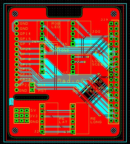
Here we start with a Raspberry Pi hat that was part of Jude Pullen's Radio Globe Project

This PCB design is an interconnection of various modules via their specific connectors to a Raspberry Pi. The Vlog presents an interesting development of the project and worth a look at the above link, but here we continue and produce a panel using this PCB as an example.
Working directly from the above PCB design files, not the Gerber plots we work through the Panel Wizard to produce the panel.
Click on the menu bar File - New, select the "Wizard" tab and then Panel Design from the list and click <OK>
NOTE. You do not require the actual design to bo open as this will be loaded during the Wizard step.

The opening screen is just an introduction, so just click <Next>
The preview on the right is the

The first step is to select which Technology file you wish to produce your panel with.
This needs to match the layers used for your PCB design. Once selected click <Next>

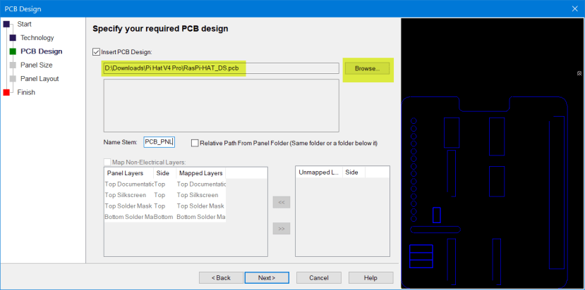
Use the "Browse" button to navigate to the Project folder and select the PCB file to be inserted into the design. Once selected a preview will appear in the right-hand pane.
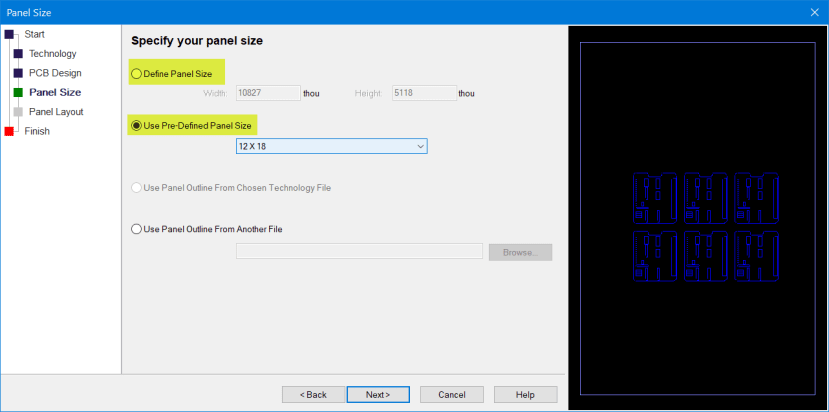
Next, we select from predefined panel sizes or define our own size.
Now we define the layout of the PCB's within the panel.
Defining the Panel Border, PCB orientation, the number of PCB in the X and Y directions and the X and Y spacing. The PCB dimensions are also listed for you to calculate your own requirements, but when you click <Next> a "panel fit" calculation is done, and an error message will be presented if the specifications do not match the Panel size.
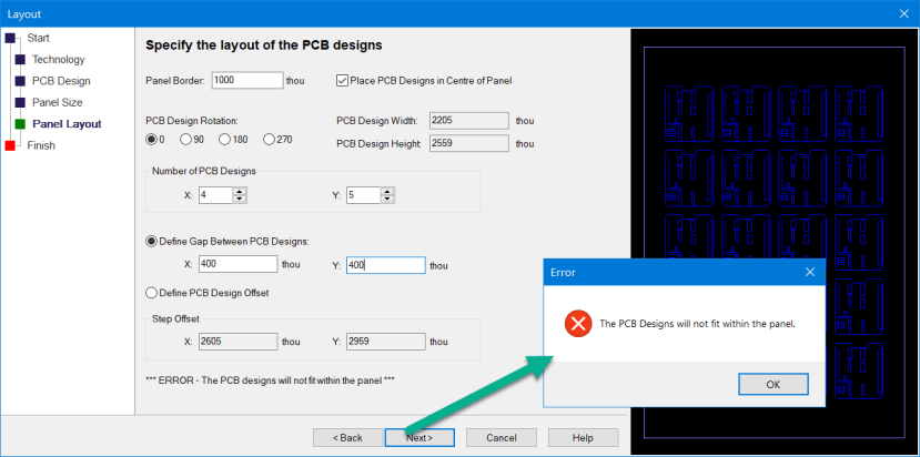
Close the error message and click the <Back> button to update your panel.
Here reducing the Panel border allows a successful design, but you may change the number of boards, orientation or spacing to meet your requirements.

At this point the panel layout is finished, clicking <Next> will display your panel.
Save this file.
Note. In this view, only certain layers are displayed to aid a visual appreciation of the layout, but all are present ready to produce the Panel Gerber plots.
Gerber plots for your panel.
The Gerber plots are produced as any normal PCB plot, however, there are a few extra settings to be aware of.
Launch the Manufacturing Outputs as normal.
Check all the required plot layers are selected and under the "Output" tab that each plot is set for plot type "Artwork" which is the default.

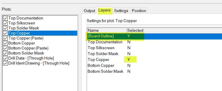
For each plot file (selected by highlighting in the left column) check on the "Layers" tab, ONLY one layer is selected, and it is the correct layer for the plot file!
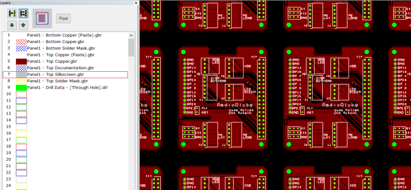
The only exception is the use of the [Board Outline] which may also be selected to add to the plot files as shown in the image below. Typically this is added to the Top copper plot.
This article discusses two methods of how to add a board outline to Gerber plots.
The above steps are common to PCB and Panel Gerber plots.
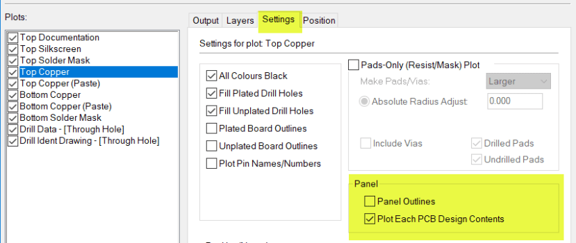
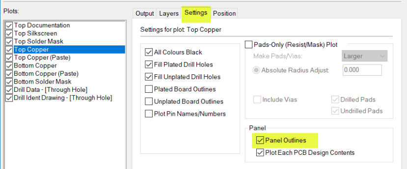
There are two additional settings when plotting a panel, for each layer plot file select the "Settings" tab and you will see these additional options.
"Plot Each PCB Design Contents" should be checked as shown.
The additional option "Panel Outlines" serves a similar function to the board outline and must be checked for at least one layer which again is normally the Top Copper layer.
Check with your manufacturer's requirements as they may require on another layer such as Top Documentation.
With everything set up Run the Plot File Generation.
A Plot File Report will be generated showing all the settings used which will show where you chose to plot the files to and also the Gerber settings which may be required to successfully import your plots into a Gerber viewer.
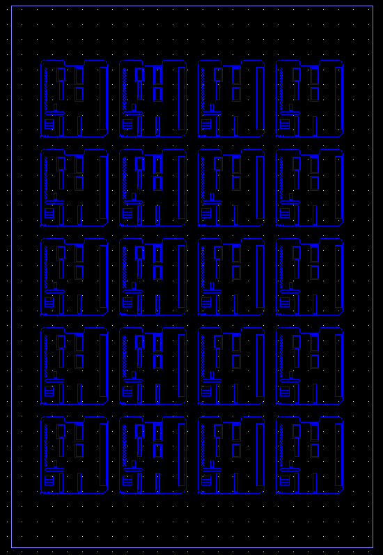
Below is an example of viewer import showing all layers.
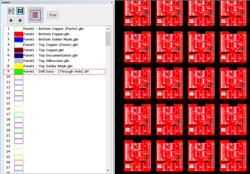
You can zoom in to see individual tracks and layers etc., but this should have all been checked at the PCB creation stage.
Your panel design is now ready for manufacture.