Panelise with DesignSpark PCB
Follow article
 Dave from DesignSpark
How do you feel about this article? Help us to provide better content for you.
Dave from DesignSpark
Thank you! Your feedback has been received.
Dave from DesignSpark
There was a problem submitting your feedback, please try again later.
Dave from DesignSpark
What do you think of this article?
Note: to use the below features, you will need DesignSpark PCB with an Engineer subscription.
Panelised Gerber output files are useful for several reasons:
- Your PCB design requires being populated with components in a batch.
- You can keep your stock as a panel and use as required.
- Multiple different PCB's for a project can be kept together.
With DesignSpark PCB and an Engineer subscription, there are two methods of producing a panelised output.
The first is via the Manufacturing Outputs that allows your PCB design to be produced as a panel. The steps are very simple.
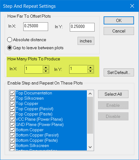
From the Manufacturing Output window select the "Step and Repeat" tab.

In the form that opens configure the output plot requirements.
Select the required plots (which is generally "All").
The spacing/offset required between the individual PCB plots.
The array of the panel.
Here you see the Preview after an array size of 4 x 3

Now click "Run" to produce the Gerber files for the panel.
Use your preferred Gerber Viewer to review the panel.

NOTES.
It is important that you review the requirements of your preferred PCB manufacture and meet their requirements. Information on the location of 'mouse bites' interconnecting the panels, panel mounting holes etc., has to be communicated to the manufacturer.
A second method is to use the "Panel Wizard"
This method makes the panel design part of the project and allows you to add layers documenting your requirements prior to producing your plots to the manufacturer.
From File - New choose the "Wizards" tab and select the "Panel Design".

Now work through the Wizard selecting your requirements.

When completed a new tab for the panel is added to your project.

New layers may be added and documented for the positioning of 'mouse bites', panel location holes, reference points etc., to aid the panel manufacture.
Key points to review against the manufacturers requirements are:
- Panel size.
- Board spacing.
- Specifying v-cuts.
- Panel slots and breakoff requirements.
- Board outline slots and perforation holes.
Due to the complexities of the options, some manufacturers also provide their own panelising tool. This allows DSPCB users also to create their own panel. For Engineer subscribers, the choice of methods are not restricted and you can choose whichever you prefer.
A further point is you may also benefit from price discounts by not panelising. If this is not an essential requirement, the manufacturer will distribute your boards across the manufacturing boards and reduce waste.
Further help on the Panel Editor and Wizard can be found in the User Guide available for DSPCB from the Help menu.