How to produce Gerber files?
Follow tutorial
 Dave from DesignSpark
How do you feel about this tutorial? Help us to provide better content for you.
Dave from DesignSpark
Thank you! Your feedback has been received.
Dave from DesignSpark
There was a problem submitting your feedback, please try again later.
Dave from DesignSpark
What do you think of this tutorial?
This tutorial requires:
DesignSpark PCB V11.0.0DesignSpark PCB provides a "Manufacturing Plots" feature to allow you to produce Gerber files and use any board manufacturer you wish.
Before producing the Gerber files, ensure you have completed all the design checks of your PCB layout to ensure you do not have errors or unexpected cost penalties from selecting nonstandard track widths or spacing or other premium features.
Producing the Gerber files.
From the menu bar select Output -> Manufacturing Plots, this will open a new window.
Select ‘Auto-Gen plots’ and then ‘Gerbers’, this will open the following view. Ensure ‘Layer/Plot Types’ and ‘Side’ are both set to ‘All’ and you also include the NC drill plot and click OK.

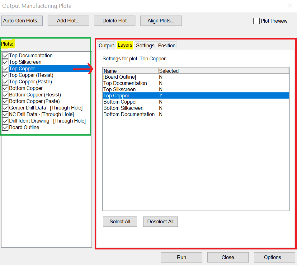
Check that all the required Plots are selected in the tick box for plotting in the left panel of main window (reselect if unchecked).
The image below explains this window further. The "Plots" ticked within the green highlighted area are the plots that will be produced. For the selected plot e.g., "Top Copper" (highlighted below) the tabs in the purple box are the settings for just that layer as per the title "Settings for plot Top Copper".
This is an important point. From the "Layers" tab ONLY the required layer should be selected to be included in that plot. You should not need to change any of these preset settings.
The exception to this is discussed below where the [Board Outline] may also be selected.
The board outline now has to included, however due to manufacturers having differing requirements on how the board outline is presented see the article “How can I add a board outline to my Gerber plots?”. We will use "Option 1" described in the above article.
NOTE: It is important that each Plot selected has only the required layer selected in the "Layers" tab for that plot. The exception is the Board Outline which can be add as described previously.
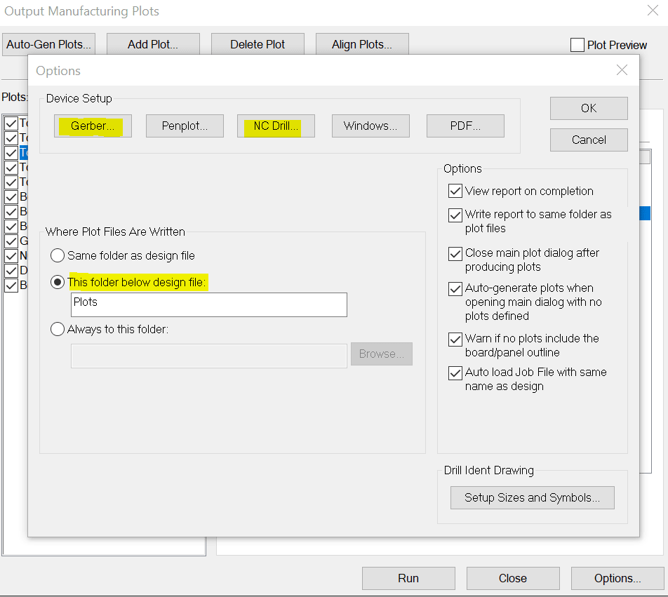
The Gerber and NC Drill settings may be changed to match your PCB and manufacturers requirements by clicking the "Options" button and then the required Gerber or NC Drill buttons in the new window.
This window also has an option to define where the plot files are written to. The default setting to a folder "Plots" within the design project is useful to keep all the related files within the project.
Suggested values for the precision and integer settings are:
Gerber 3:5
NC Drill 2:3
With all the setup completed now all that is required is to press the "Run" button.
A report file will be produced which should be checked to ensure everything was correct and the Gerber files will be written to the "Plots" folder. These should now be examined with a Gerber viewer to ensure all is correct.
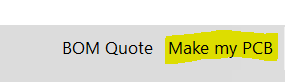
Our DesignSpark service partners can help you find a suitable manufacturer for your specific PCB requirements and assist with the process. This facility is available from the "Make my PCB" at the top right of DesignSpark PCB.
Depending on your manufacturer you may have to rename the Gerber layer name and file extension to a format to meet specific requirements. This can be achieved in the normal Windows file manager.
Notes:
The Drill Ident plot is to identify drill holes by a symbol, it is not physically part of the board so should be disabled in the Gerber viewer to avoid confusion.
If you have used any features such as slotted holes or V-cuts in your design and defined on the documentation layer, please bring this to the attention of your board manufacturer to ensure your requirements are met.