Introduction to Ideal Op-Amp Circuit Characteristics
Follow articleHow do you feel about this article? Help us to provide better content for you.
Thank you! Your feedback has been received.
There was a problem submitting your feedback, please try again later.
What do you think of this article?
Introduction
Operational amplifier (op amp for short) is basically a voltage amplifying device designed to be used with components like capacitors and resistors, between its in/out terminals, or is simply a linear Integrated Circuit (IC) having multiple-terminals. In electronics, the open-loop voltage gain of the actual operational amplifier is very large, which can be seen a differential amplifier with infinite open loop gain, infinite input resistance and zero output resistance. In addition, it has positive and negative inputs which allow circuits that use feedback to achieve a wide range of functions. And meanwhile, it can be further simplified into an ideal op amp model, referred to as an ideal op amp (also called ideal OPAMP).
1 Ideal Op Amp Characteristics
When analyzing various application circuits of operational amplifiers, the integrated operational amplifier is often regarded as an ideal operational amplifier. The so-called ideal op amp is to idealize various technical indicators of op amps, and it must have the following characteristics.
1.1 Infinite Input Resistance
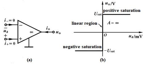
The input terminal of an ideal operational amplifier does not have any current to flow in. In electronics, op amps are voltage gain devices. They amplify a voltage fed into the op amp and give out the same signal as output with a much larger gain. In order for an op amp to receive the voltage signal as its input, the voltage signal must be dropped across the op amp. If you know the concept of a voltage divider, voltage drops primarily across components with high impedances, proportionally according to ohm’s law by the formula V=IR. So the greater the resistance (or impedance) of a device, the greater the voltage drop across that device is. To make sure that the voltage signal drops fully on the op amp, it must have a very high input impedance, so that the voltage drops fully across it. If it had a low input impedance, the voltage may not drop across it and it would not receive the signal. This is why op amps must have high-input impedances.
It’s also easy to make the input impedance lower (put a resistor in parallel) or the source impedance higher (put a resistor in series).
Figure 1. Ideal Op Amp Symbol and Transfer Characteristic Curve
1.2 Zero Output Impedance
The output of an ideal op amp is a perfect voltage source, no matter how the current flowing to the amplifier load changes, the output voltage of the amplifier is always a certain value, that is, the output impedance is zero. In practice, zero output impedance is actually a distinct property from infinite input impedance, but for a very long time infinite input impedance was approached only with compromises in offset voltage and noise.
1.3 Infinite Open-loop Gain
In an open-loop state, the differential signal at the input has an infinite voltage gain. This feature makes the operational amplifier very suitable for practical applications with upper negative feedback configuration.
1.4 Infinite Common-mode Rejection Ratio
An ideal operational amplifier can only respond to the difference between the voltages at both ends of V+ and V-. In addition, the same part of the two input signals (ie common mode signal) will be completely ignored. What’s more, a high CMRR is required when a differential signal must be amplified in the presence of a possibly large common-mode input, such as strong electromagnetic interference (EMI). An example is audio transmission over balanced line in sound reinforcement or recording.
1.5 Infinite Bandwidth
The ideal operational amplifier will amplify the input signal of any frequency with the same differential gain, which will not change with the change of signal frequency.
2 Assumptions of Ideal Op Amp
The op amp can be considered a voltage controlled current source, or it is an integrated circuit that can amplify weak electric signals. Based on it, for an ideal OPAMP, what is the relationship between it and these electrical signals?
First, assume that the current flowing into the input of the op amp is zero. This assumption is almost completely correct for FET op amps, because the input current for FET op amps is below 1pA. But for dual high-speed op amps, this assumption is not always correct, because the input current of it can sometimes reach tens of microamperes.
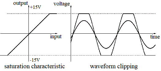
Second, assume that the gain of the op amp is infinite, so the op amp can swing the output voltage to any value to meet the input requirements. It means that the output voltage of the op amp can reach any value. In fact, when the output voltage is close to the power supply voltage, the op amp will saturate. Maybe this hypothesis does exit, but needs a limit in practical. For example, at higher frequencies, the internal junction capacitors of transistor come into play, thus reducing the output and therefore the gain of amplifier. The capacitor reactance decreases with increase in frequency bypassing the majority of output. The opamp is in saturation state.
Figure 2. Op Amp Saturation
For example, as per datasheet of LM741, large signal voltage gain is 200V/mv. It means an open loop gain of 200,000. If you operate an op-amp in open-loop condition(i.e. without negative feedback) ,even microvolts of input voltage (input offset voltage of LM741 is 3mv) will drive the output to saturation.
In most of the amplifier circuits op-amp is configured to use negative feedback which greatly reduces the voltage gain (i.e. closed loop gain). In oscillators and schmit triggers, Op-amp is configured to use positive feedback. Comparator circuit is an example of the circuit which utilizes open-loop gain of op-amp. Its output will be always at saturation either positive or negative saturation. In an integrator circuit, the DC gain should be limited by adding a feed back resistor in parallel with capacitor ;else the output will get saturated .
Even in amplifier circuits, the amplitude of the input signal and the voltage gain of the circuit should be balanced so that the output voltage does not exceed power supply voltage . For example for a non-inverting amplifier with a voltage gain of 100, the maximum permissible input voltage will be 150 mv if the VCC is 15 Volts. If you apply a signal of 200 mv ,the op-amp output will goto saturation as the required output will be 20 volts which exceeds the VCC of 15 Volts.
Third, the assumption of infinite gain also means that the input signal must be zero. The gain of the op amp will drive the output voltage until the voltage (error voltage) between the two input terminals is zero. The voltage between the two input terminals is zero. The zero voltage between two input terminals means that if one input terminal is connected to a hard voltage source like ground, the other input terminal will also be at the same potential. In addition, since the current flowing into the input terminal is zero, the input impedance of the op amp is infinite.
Fourth, of course, the output resistance of an ideal op amp is zero. An ideal op amp can drive any load without any voltage drop due to its output impedance. At low currents, the output impedance of most op amps is in the range of a few tenths an ohm, so this assumption is true in most cases.
3 Working Characteristics of Ideal Operational Amplifiers
3.1 Work in Linear Region
When the ideal op amp works in the linear region, the output and the input voltage show a linear relationship. Where u0 is the output voltage of the integrated op amp; u+ and u- are the voltages at the non-inverting input terminal and the inverting input terminal, respectively. Auo is the open loop differential voltage magnification. According to the characteristics of the ideal op amp, two important characteristics of the ideal op amp in the linear region.
1) Zero differential input voltage
Since the open-loop differential voltage magnification of an ideal op amp is equal to infinity, and the output voltage is a certain value, the voltage values at the non-inverting input terminal and the inverting input terminal are approximately equal. Just like short circuit between input and output, but it is fake. Because it is an equivalent short circuit, not a real short circuit, so this phenomenon is called "virtual short".
2) Zero input current
Since the open-loop input resistance of an ideal op amp is infinite, no current flows into the op amp at either input. At this time, the current at the non-inverting input terminal and the inverting input terminal are both equal to zero. Like an disconnection, but an equivalent disconnection, so this phenomenon is called "virtual break". Virtual short and virtual break are two important concepts for analyzing the ideal op amp working in the linear region.
In fact, the ideal operational amplifier has the characteristics of "virtual short" and "virtual break". These two characteristics are very useful for analyzing linear amplifier circuits. The necessary condition for virtual short is negative feedback. When negative feedback is introduced, at this time, if the forward terminal voltage is slightly higher than the reverse terminal voltage, the output terminal will output a high voltage equivalent to the power supply voltage after the amplification of the op amp. In fact, the op amp has a respond time changing from the original output state to the high-level state (the golden rule of analyzing analog circuits: the change of the signal is a continuous change process). Due to the feedback resistance of the reverse end change will inevitably affect its voltage, when the reverse end voltage infinitely close to the forward end voltage, the circuit reaches a balanced state. The output voltage does not change anymore, that is, the voltage at the forward end and the reverse end is always close. (Note: The analysis method is the same when the voltage decreases.)
3.2 Work in Nonlinear Region
When the op-amp operates in the nonlinear region, the output voltage no longer increases linearly with the input voltage, but saturates. The ideal op amp also has two important characteristics when operating in the nonlinear region.
1) When u+ ≠ u-, the output voltage of the ideal op amp reaches the saturation value.
When u+ > u-, the op-amp operates works in positive saturation region with a positive output voltage.
When u+ < u-, the op-amp operates works in negative saturation region with a negative output voltage.
Ideal op amp operates in the nonlinear region, u+ ≠ u-, there is no “virtual short”.
2) The input current is equal to zero.
Although the input voltage u+ ≠ u- above, the input current is considered to be zero.
4 Characteristics Analysis of Ideal Operational Amplifier
As for Op-amp, there's probably a description like this: three-terminal element (circuit structure with double-ended input, single-ended output), ideal transistor, high-gain DC amplifier.
(1) High input resistance
Under this situation, the current flowing into the input terminal is close to 0, almost no signal source current is used, which is close to the voltage control characteristic. And virtual break is derived from this.
(2) Lower output resistance
It has the characteristics of adapting to any load. And the impedance of the subsequent load circuit will not affect the output voltage.
(3) Infinite voltage amplification
(4) Under a certain supply voltage condition, the amplifier can only work in closed-loop (negative feedback) mode, and the actual amplification is limited. Because op-amps themselves don't have a 0V connection but their design assumes the typical signals will be more towards the center of their positive and negative supplies. Thus, if your input voltage is right at one extreme or forces the output toward one supply, chances are it won't work properly. Working in open-loop mode is the like a comparator, and the output is high level or low level.
In the closed-loop (limited amplification) state, the amplifier is randomly compare the potentials of the two input terminals. The output stage makes immediate adjustments when they are not equal. So the final purpose of amplification is to make the potentials of the two input terminals equal. And virtual short is derived from this.
5 Balanced Resistance Presets
5.1 The Role of Balanced Resistance
1) A suitable resistance is generally required to ensure that the input impedance is matched.
2) In order to reduce the input current imbalance, the in-phase resistor should be equal to the parallel value of the two resistors at the reverse end in theory. In practice, as a result of the closed loop, especially in deep negative feedback conditions, the misalignment is not obvious at the output. And there is no need of in-phase grounding resistor when the misalignment is not the main problem. Because a balanced resistor is the starting point for an ideal op amp. In-phase grounding resistance is useful for bipolar op amps, and has no meanings for MOS-type op amps.
3) Ground input termination resistance: it is necessary for impedance matching and high frequency setting.
4) Bias current and offset current.
For operational amplifiers with bias current greater than offset current, input resistance matching can be reduced, and precision circuits can compensate bias current to a minimum. If the bias current and offset current are similar, the matching resistance will increase the error.
5) Set for the bias current at the input, the purpose of which is to equalize the impedance of the inverting and non-inverting inputs, so that two inputs with equal bias currents are assumed to have equal voltage drops, thereby counteraction can be made.
5.2 Input Balancing Resistor Explanation
A op-amp is connected to an inverting amplifier:
Set the input resistance for R1, feedback resistance for Rfi,
Assume that the non-inverting end is not connected to a balanced resistor, but grounded directly.
Set the input bias current for the op-amp IB (same voltage in inverting and non-inverting end).
The current flows through R1 and Rf are represented by I1 and If.
Inverting voltage is V-, The op-amp gain is A.
Use KCL in the inverting end (set the input signal to 0).
Where (0-V-)/R1- (A+1)V- /Rf=IB
From the above equation, it follows that V-=-(IB×R1×Rf/(Rf+(A+1)R1))
At this time, the output voltage of the op-amp is Vo=A×(IB×R1×Rf/(Rf+(A+1)R1))<
The above formula can be approximated as Vo=IB×((A×R1)/Rf)
If the in-phase terminal passes through a resistor R2 to ground and R2=R1/Rf, then the voltage at the in-phase terminal is V+=-IB×R2
KCL is applied to the inverted terminal, where (0-V-)/R1+(A×(V+-V-)-V-)/Rf=IB
>At this time the output voltage of the op-amp is Vo=0.
6 Ideal Op Amp Equations
Understanding the basic conditions of an ideal op amp, and combining it with the Kirchhoff's current law (KCL) node voltage method and the superposition theorem of the node, is an effective method to analyze the ideal op amp circuit.
As shown below, find the output voltage uo
1) Equation based on KCL
From the concept of virtual break, i+=i-=0, then i1=i2, i3=i4, so

Based on virtual break, u+=u-, then

2) Node voltage method
List the node voltage equations for node 1 and node 2, and get

Note: Because the output current of the op amp is unknown at 1) and 2), it is not possible to list the KCL equation or node voltage equation at the output of the op amp. In addition, the op amp output uo in 2) should be treated as an independent voltage source.
3) Superposition theorem
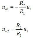
When there are multiple signal inputs, choosing the superposition theorem to solve can simplify the analysis and calculation process. The size of the output signal uo can be regarded as the superposition of the output signal obtained by the independent action of u1 and u2. When u1 acts alone, the u2 terminal is grounded, and the op amp output is:

Therefore, the final output of the operational amplifier is:

7 Several Common Op Amp Circuits
Non-inverting Amplifier Circuit
A non-inverting amplifier is an op-amp circuit configuration which produces an amplified output signal. It provides a high input impedance along with all the advantages gained from using an operational amplifier.
Figure 3. Non-inverting Amplifier Circuit
Inverting Amplifier Circuit
An inverting amplifier (also known as an inverting operational amplifier or an inverting op-amp) is a type of operational amplifier circuit which produces an output which is out of phase with respect to its input by 180 degrees out of phase with respect to input signal. In the following figure, two external resistors to create feedback circuit and make a closed loop circuit across the amplifier.
Figure 4. Inverting Amplifier Circuit
Op-amp as Adder
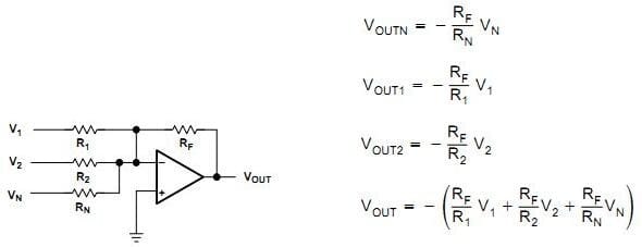
An adder circuit can be made by connecting more inputs to the inverting op amp. The circuit diagram of a summing amplifier is as shown in the following figure.
Figure 5. Op-amp as Adder
Differential Amplifier
Differential amplifier is an analog circuit with two inputs and and one output in which the output is ideally proportional to the difference between the two voltages. It is a very useful op-amp circuit and by adding more resistors in parallel with the input resistors as shown in the following.
Figure 6. Differential Amplifier
Composite Amplifier
The composite amplifier is termed as a combination of multiple operational amplifiers that are cascaded together with a negative-feedback loop around the entire network.
Figure 7. Composite Amplifier
The resistance in the circuit is generally selected at the K ohm level, the ratio of the resistance affects the gain and bias, in addition, the supply current, frequency response and capacitive load driving capability of the op amp determine their specific values in circuits. If it is used in a high-frequency circuit, the resistance needs to be reduced to obtain a better high-frequency response, but it will increase the input bias current, thereby increasing the current of the power supply.
8 Difference Between Ideal Op-amp and Practical Op-amp
Ideal op amps use no power, have infinite input impedance, unlimited gain-bandwidth and slew rate, no input bias current, and no input offset. They have unlimited voltage compliance.
Practical op amps consume some power, have very high input impedance have limited gain-bandwidth and limited slew rate, have some input bias current and input offset voltage. Voltage compliance is limited by the power supply rail, or frequently even less.
Still practical op amps are very useful because most of the limitations listed above are way better than what your circuit needs.
For an ideal amplifier, it does not draw any current at all from its input. Assuming a two input amplifier the signal current in both input probes is zero. In other words the input impedance must be infinite. The output, should operate as the output of an ideal voltage source. This means that the potential between the output and the ground must be A(v2−v1), no matter how much current would a load connected to the output would draw. In other words the output impedance must be zero.
For a real amplifier, the input impedance must be as large as possible while the output impedance must be as low as possible.
In fact, An op-amp in real life, however, cannot operate with zero current flow.
9 Reference
Electronic Operational Amplifier Basics Overview
Non-Inverting and Inverting Amplifiers Basics Overview
Core Problems Analysis of Operational Amplifier Basics


