A Look at the ST 3.6kW SiC PFC Totem Pole Reference Design Board
Follow articleHow do you feel about this article? Help us to provide better content for you.
Thank you! Your feedback has been received.
There was a problem submitting your feedback, please try again later.
What do you think of this article?
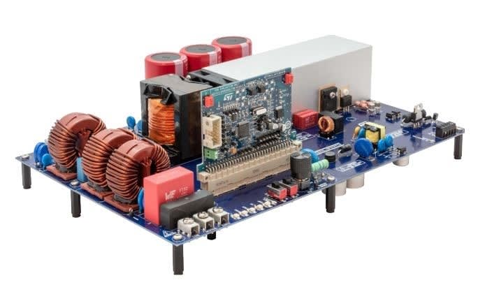
Exploring silicon carbide MOSFET technology advantages, PFC and the STEVAL-DPSTPFC1 reference design board (215-0834) .
Introduction
In this article, we’ll be discussing what silicon carbide MOSFETs are, the advantages of them and then finally taking a look at the STEVAL-DPSTPFC1 reference design that utilises SiC devices to provide power factor correction.
What are Silicon Carbide MOSFETs?
Silicon Carbide MOSFETs are switching devices much like common Silicon MOSFET devices, with some advantages gained from using a silicon carbide semiconductor material. SiC devices are designed, processed and produced much like silicon devices, meaning the cost for the device performance is roughly comparable with silicon parts.
Where the differentiation begins is in the advantages that SiC devices present — the higher junction operating temperature compared to silicon devices, on the order of 200°C versus a typical 150°C means the devices can be pushed harder; a higher blocking voltage on the drain-source junction — ST offer devices with a breakdown voltage of up to 1700V for even the most demanding applications; lower switching losses with minimal temperature variation for applications that need to switch at high frequencies; and low on-state resistance that remains steady over the device operating temperature range.
These advantages make SiC devices a strong contender to replace traditional silicon devices, especially given the lower switching losses and low on-state resistance that remains steady — meaning that a higher power handling capacity can be packed into the same area as what would be possible with silicon devices.
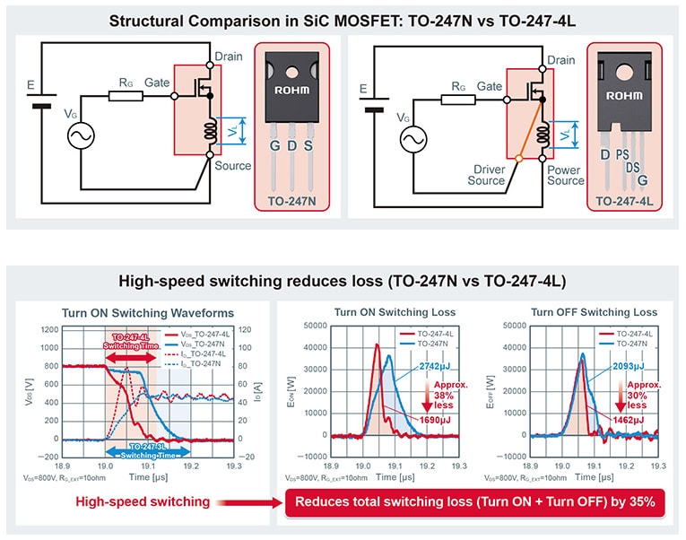
Often, SiC MOSFETs include an extra source pin on the package and differentiate between the two as a power source and driver source. This extra source pin allows for the driver return current to get to the MOSFET source quicker (thanks to the minimised parasitic inductance), further improving the switching speed of a SiC device.
SiC devices are commonly targeted at applications requiring high power, high-performance semiconductors, such as electric vehicle on-board converters, photovoltaic inverters, power conversion and industrial drives, variable frequency drives, traction applications, high voltage DC power supplies and EV charging stations — often where space is a premium, and a high power density is needed.
Why is PFC Necessary?
Power factor correction (PFC) is necessary especially for larger electrical loads such as large switch-mode power supplies, motors and drives. To give a bit of background, the power factor is the ratio of working power (measured in watts) to the apparent power (measured in volt-amperes).
An ideal power factor has a value of 1.0 — common of resistive loads such as incandescent light bulbs or resistive heaters. A load with a power factor of less than 1.0 causes losses in a power distribution system, leading to increased distribution equipment load and costs associated with supplying energy. Therefore making only a minor improvement to power factor can have a significant reduction in losses, since the losses are proportional to the square of the current.
One example that nicely demonstrates the power factor and the effects is a single-phase motor. The magnetising current of the motor is not in phase with the voltage; this current phase difference is what causes the motor shaft to rotate. It is worth noting that the magnetising current does not contribute to the useful work output of the motor, so the benefit of improving the power factor can immediately be seen.
For example, the single-phase motor could have a current draw of 10A with a power factor of 0.75, making the useful current 7.5A. Therefore, the total useful power from the motor is 230V x 7.5A = 1.725kW, meaning that there is 2.5A left that is not contributing to the useful power output, and the same 10A has to be supplied.
Adding a power factor correction system to a motor could therefore reduce the total current draw of the motor by modifying the current phase with respect to the voltage. The IET has a paper that looks in more detail at power factor correction, and how power factor can be improved.
Large consumers, such as factories, could potentially be billed higher if they present a poor power factor to the grid. Some energy suppliers might even offer incentives in the form of lower energy prices if a consumer can have a good power factor, typically above 0.9 to 0.95.
The Hardware
Reference Design Kit
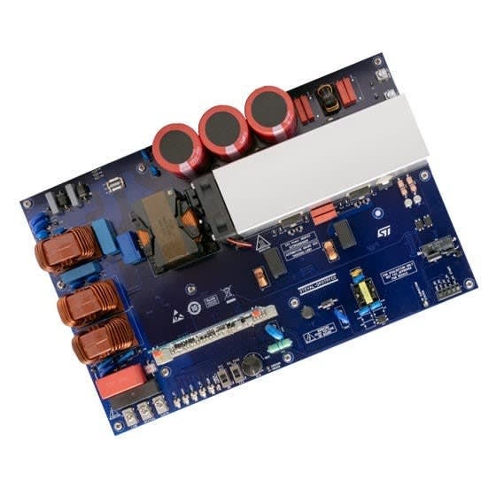
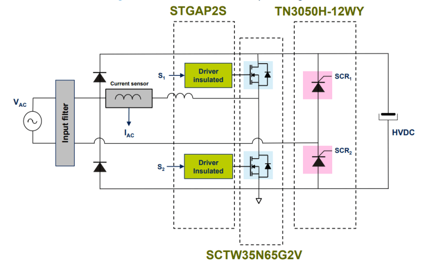
The STEVAL-DPSTPFC1 reference design kit (215-0834) includes everything necessary to get started evaluating ST’s SiC MOSFETs in a PFC application. On-board there are all the necessary components to do inrush current limiting and PFC, including the two SiC MOSFETs, two SCRs and all other supporting componentry.
SiC MOSFETs provide the power factor correction switching, which is where most of the power would normally be dissipated, as this section runs continuously to supply the high voltage DC output; and then thyristor SCRs are used to handle the inrush current limiting.
A flyback power supply is also provided to generate the necessary voltage rails on the board, including two isolated supplies for the SCRs and an isolated supply which supplies the microcontroller, current sensor and other control circuits, and additionally feeds two isolated MOSFET drivers.
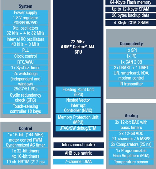
Also included in the kit is a microcontroller board containing an STM32F334 (196-2026) . The STM32F3x4 series of microcontrollers is specifically designed with features targeting digital power conversion applications including D-SMPS, lighting systems, welding, inverters for photovoltaic systems and wireless chargers.
Notable features of the STM32F3x4 line of microcontrollers include a high-resolution timer subsystem consisting of six timers capable of a 217ps interval, with ten PWM outputs (that can be coupled into pairs), ten external event inputs (such as current limit, zero voltage/zero current detection) and five fault inputs.
Three ultra-fast comparators are also included that take only 26ns from analogue input to PWM shutdown — useful for implementing a hardware overcurrent or overvoltage shutdown. Additionally, an op-amp with five built-in selectable gain settings is also included, boasting a 1% accuracy.
Board Specifications
The STEVAL-DPSTPFC1 reference design kit (215-0834) has a rated input of 85-264VAC 45-65Hz, and is capable of pulling up to 16A/3.6kW from the mains input — this is worth noting if you opt to evaluate the board using a standard UK plug to supply power as the maximum supply current is only 13A. The maximum output from the board is 420VDC at 9A, with a 230V AC input — the output current is roughly halved at 110VAC to 4A, as is to be expected.
The PFC circuit on-board features a high power factor of at least 0.99 across the tested input range of 110-240VAC 50/60Hz, and the efficiency figures are similarly as impressive - at least 92% efficient with an input of 110VAC 60Hz.
Total harmonic distortion figures are equally as good, with the lowest THD figure of 3.5% at 230V 50Hz.
Board Operation
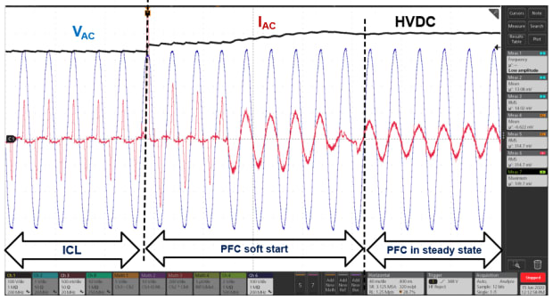
The board operation consists of a number of discrete steps to provide inrush current limiting, and soft starting of the PFC circuit to reduce component stress and to limit the PFC inrush current.
Inrush current limiting should be implemented on equipment with a rated RMS input current of below 16A to be compliant with the IEC 61000-3-3 standard — this sets out limitations for the voltage changes and fluctuations caused by inrush currents, which can cause unwanted flicker or brightness variations in lighting and displays.
Typically, inrush current is implemented with two relays and an NTC resistor that limits the initial inrush current and is then shorted by one of the relays. This is a somewhat inefficient way of performing inrush current limiting, and over time the resistance of the NTC resistor increases with each cycle — further hurting the efficiency of the current limiting circuit.
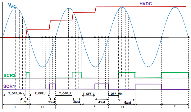
The above image demonstrates how the SCR circuit performs inrush current limiting, by progressively charging the HVDC bus capacitance to the peak voltage of the AC waveform.
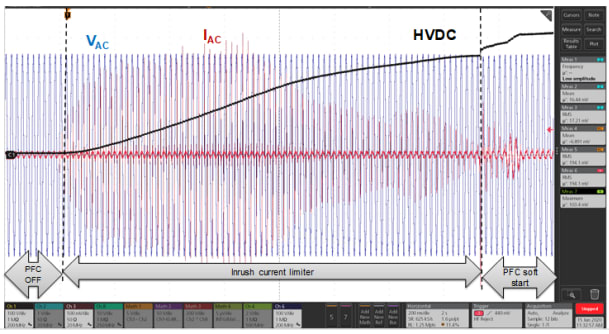
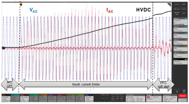
The firmware provided by ST implements two different selectable methods of inrush current limiting: fixed SCR on delay, and variable SCR on delay. Fixed SCR on delay involves keeping the delay that the SCR is turned on for a fixed value or a multiple of, leading to higher current peaks on the 230V input that can vary from cycle-to-cycle.
Variable SCR on delay involves changing the on-delay of the SCR devices according to a lookup table, which takes into account a model of the AC line voltage input. This results in a lower average line current, with current peaks that average the same cycle-to-cycle value.
After the inrush current limiting procedure has ended, the PFC controller is then engaged to take the HVDC bus to the final 400VDC output voltage.
The PFC soft-start management routine is executed at every zero crossing of the AC input, to gently bring up and then regulate the HVDC bus.
With the inrush current limit and PFC soft-start completed, the PFC controller is then running in a steady-state mode. This includes controlling a current spike that is present at the zero-voltage crossing of the AC input, overcurrent protection utilising the on-chip DAC & comparators, PFC choke inductor current clamping and HVDC overvoltage protection.
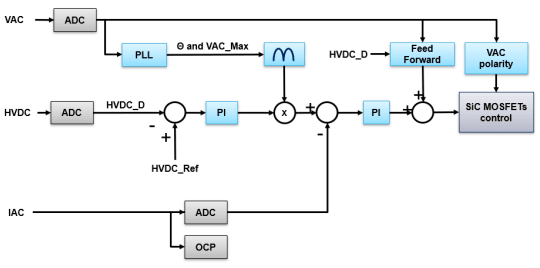
Two control loops plus a phase-locked loop provide the digital control system. An outer voltage loop is responsible for regulating the HVDC output voltage, and a faster current control loop oversees shaping the PFC inductor current to the AC supply sine wave. Finally, the PLL is responsible for keeping the entire PFC control loop synchronised to the mains cycle.
Control Loop Design
Control loop design is no easy task, but ST has made the process substantially easier for this particular task by providing a full breakdown of the controller design in the user manual.
The user manual also covers the theory of operation in much greater detail and includes full schematics and component choices used on the STEVAL-DPSTPFC1 reference design.
To Finish
In this post we have taken a look at what SiC MOSFET devices are, and why they are a desirable choice for high voltage, high power applications, why power factor correction is important and an example of power factor, and finally the ST STEVAL-DPSTPFC1 reference design for a 3.6kW PFC totem pole.


Comments