Wireless Power Transfer System for Rehabilitation - 1st Prototype Development
Follow article Dave from DesignSpark
How do you feel about this article? Help us to provide better content for you.
Dave from DesignSpark
Thank you! Your feedback has been received.
Dave from DesignSpark
There was a problem submitting your feedback, please try again later.
Dave from DesignSpark
What do you think of this article?
This article is the second part of 'Wireless power transfer system for rehabilitation' and details the development of the first prototype of the system, built to test the components and gain an idea of the wireless power transfer system.
Development Log
Part 1: Motor Driver and MCU Testing
As mentioned previously, the transmitting side will be built as the basic structure first.

Choosing the ‘right’ components is a key part of the project. At this point, the reason for choosing STM32F407VG Discovery as the MCU is that STM32F407VG is a general-use and easy-to-use MCU. The Discovery Board is easier to handle than a chip STM32 MCU. A motor driver DRV8412 is used since it is also an easy-to-use component. DRV8412 includes 2 full-bridge (or 4 half-bridge) inside the IC. Once the MCU sends serval PWM signals to the driver, the driver can output AC power to drive the coils. And also, there are error protections built in the IC, including Under-voltage protection, Overcurrent Protection, Overtemperature Protection and Device Protection System. Those features of the DRV8412 driver make the IC easy to implement and friendly for beginners.

The system is built similarly with the application example from the datasheet of DRV8412. To make the system more flexible and universal, the M1, M2, and M3 (mode selection pins) are connected to the MCU.
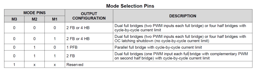
In our application, Dual full bridges are designed. Then the mode selection pins should be 000.
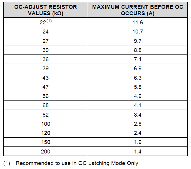
In the above diagram, the value of the Roc_adj will determine the Overcurrent (OC) threshold. In the project, 150kΩ Roc_adj is used.

This is the schematic diagram of the system. The PCB Layout will be like the image shown below.

This is the PCB layout for the system. After adding the ground plane and vias, the layout is ready to print out. Please make sure that the wires of outputs are wide enough. “Pour copper shape” is used in the design to draw the wider wire for the outputs.

This is the product of the system. And it is ready for use.
Components list
|
Item |
Unit |
RS Stock No. |
|
Texas Instruments DRV8412DDW, Brushed Motor Driver IC |
1 |
|
|
Discovery Kit for STM32F407VG Microcontroller |
1 |
|
|
LDO Regulator Pos 5V 1A Microchip MIC39100-5.0WS |
1 |
|
|
Nichicon 220F 50 V Aluminium Electrolytic Capacitor SMD |
4 |
|
| Panasonic Aluminium Electrolytic Capacitor 330μF 16 V |
1 |
|
| AVX 470nF Multilayer Ceramic Capacitor MLCC 16 V dc |
1 |
|
| Murata 1μF Multilayer Ceramic Capacitor MLCC 16 V dc |
5 |
|
| TDK 22μF Multilayer Ceramic Capacitor MLCC 10 V dc |
1 |
|
| Murata 47μF Multilayer Ceramic Capacitor MLCC 16 V dc |
1 |
|
|
KEMET 100nF Multilayer Ceramic Capacitor MLCC 16 V |
10 |
|
| Panasonic ERJ6RQ Series Thick Film Low Ohmic Surface Mount Fixed Resistor 0805 Case 1Ω |
1 |
|
| TE Connectivity CPF Series Precision Thin Film Surface Mount Fixed Resistor 0603 Case 15kΩ |
1 |
|
|
2 way PCB screw terminal,5mm pitch 2 way PCB screw terminal,5mm pitch |
2 |
|
|
TE Connectivity AMP QUICK Series, 2.54mm Pitch 2 Way 1 Row Straight PCB Header, Solder Termination |
3 |
Software
Then, it is time for the software part.
To program the STM32F407 Discovery Board, Keil is used as the tool. Keil can be downloaded from http://www.keil.com/.
Step 1: Go to http://www.keil.com/
Step 2: Click “Download” on the header bar
Step 3: Click on “Product Downloads”
Step 4: Select “MDK-Arm”
Step 5: Type in the information and “Submit”
Step 6: Download and install the MDK-Arm software
Step 7: Open Keil and the pack installer
Step 8: Download “Keil::STM32F4xx-DFP”, “ARM::CMSIS”, “Keil::ARM_Compiler”, “Keil::MDK-Middleware”;
(Version 1.0.8 Keil::STM32F4xx-DFP, version 5.0.1 ARM::CMSIS, version 1.3.0 Keil::ARM_compiler, version 7.4.0 Keil::MDK-Middleware are used in this project.)
(Some examples can be downloaded in pack installer which also help to learn the Discovery Board.)
Step 9: Open a project, Select “STMicroelectronics” -> “STM32F4 Series” -> “STM32F407” -> “STM32F407VG”
Then Keil is ready to use.
The program
#include "stm32f4_discovery.h"
#include <stdio.h>
#include <stm32f4xx_usart.h>
#include "stm32f4xx.h"
#include "stm32f4xx_tim.h"

/* ------------------------- Private typedef --------------------------------*/
GPIO_InitTypeDef  GPIO_InitStructure;
USART_InitTypeDef USART_InitStructure;
SPI_InitTypeDef  SPI_InitStructure;
TIM_OCInitTypeDef  TIM_OCInitStructure;
TIM_BDTRInitTypeDef TIM_BDTRInitStructure;
TIM_TimeBaseInitTypeDef  TIM_TimeBaseStructure;

/*-------------------------- Initial Timer 1 and Timer 2 --------------------*/
void init_timer1_timer2(){
	RCC_APB2PeriphClockCmd(RCC_APB2Periph_TIM1,ENABLE);
	RCC_APB2PeriphClockCmd(RCC_APB1Periph_TIM2,ENABLE);
	//The clocks of different timers are different.
	//Timer 1, 8 9-11 are using APB2, Timer 2-5, 12-14 are using APB1.
	//The frequency of APB2 is 168MHz, and frequency of APB1 is 84MHz.
	//To calculate the value of TIM_Period:
	//			PWM_frequency = clock of timer(84MHz or 168MHz) / (TIM_Period +1)
	//			TIM_Period = clock of timer / PWM_frequency - 1
	//e.g.  to set the PWM frequency as 150kHz
	//			TIM_Period for timer 1 = 168MHz / 150kHz - 1 = 1119
	//			TIM_Period for timer 2 = 84MHz / 150kHz - 1 = 559

	TIM_TimeBaseStructure.TIM_Period = 1119 ;
  TIM_TimeBaseStructure.TIM_Prescaler = 0;
  TIM_TimeBaseStructure.TIM_ClockDivision = TIM_CKD_DIV1;
  TIM_TimeBaseStructure.TIM_CounterMode = TIM_CounterMode_Up;
	TIM_TimeBaseStructure.TIM_RepetitionCounter = 0;

  TIM_TimeBaseInit(TIM1, &TIM_TimeBaseStructure);

	TIM_TimeBaseStructure.TIM_Period = 559;
	TIM_TimeBaseInit(TIM2, &TIM_TimeBaseStructure);

	TIM_CtrlPWMOutputs(TIM1, ENABLE);
	TIM_CtrlPWMOutputs(TIM2, ENABLE);
}

/*-------------------------- Generater 4 PWM signals ------------------------*/
void init_PWM_ABCD(){
	TIM_OCInitStructure.TIM_OCMode = TIM_OCMode_PWM2;
	TIM_OCInitStructure.TIM_OutputState = TIM_OutputState_Enable;
	TIM_OCInitStructure.TIM_OutputNState = TIM_OutputNState_Enable;
	TIM_OCInitStructure.TIM_OCPolarity = TIM_OCPolarity_Low;
	TIM_OCInitStructure.TIM_OCNPolarity = TIM_OCNPolarity_High;
	TIM_OCInitStructure.TIM_OCIdleState = TIM_OCIdleState_Set;
	TIM_OCInitStructure.TIM_OCNIdleState = TIM_OCNIdleState_Reset;

	//To defind the duty cycle of each channel of each timer.
	//Channel 1 & 2 of Timer 1 & 2 are used in the system.
	//TIM_Pulse = (TIM_Period + 1) * %duty cycle - 1;
	//e.g.	to set the PWM with 25% duty cycle
	//			TIM_Pulse for timer 1 = (1119+1) * 0.25 - 1 = 279
	//			TIM_Pulse for timer 2 = (559+1) * 0.25 - 1 = 139

	TIM_OCInitStructure.TIM_Pulse = 279;
	TIM_OC1Init(TIM1, &TIM_OCInitStructure);
	TIM_OC1PreloadConfig(TIM1, TIM_OCPreload_Enable);

	TIM_OCInitStructure.TIM_Pulse = 279;
	TIM_OC2Init(TIM1, &TIM_OCInitStructure);
	TIM_OC2PreloadConfig(TIM1, TIM_OCPreload_Enable);

	TIM_OCInitStructure.TIM_Pulse = 139;
	TIM_OC1Init(TIM2, &TIM_OCInitStructure);
	TIM_OC1PreloadConfig(TIM2, TIM_OCPreload_Enable);

	TIM_OCInitStructure.TIM_Pulse = 139;
	TIM_OC2Init(TIM2, &TIM_OCInitStructure);
	TIM_OC2PreloadConfig(TIM2, TIM_OCPreload_Enable);
}

/*-------------------------- Initial output PWM pins  -----------------------*/
void init_PWM_ABCD_pins(){
	RCC_AHB1PeriphClockCmd(RCC_AHB1Periph_GPIOB, ENABLE);
	RCC_AHB1PeriphClockCmd(RCC_AHB1Periph_GPIOE, ENABLE);

	GPIO_PinAFConfig(GPIOB, GPIO_PinSource10, GPIO_AF_TIM2);
	GPIO_PinAFConfig(GPIOB, GPIO_PinSource11, GPIO_AF_TIM2);
	GPIO_PinAFConfig(GPIOE, GPIO_PinSource9, GPIO_AF_TIM1);
	GPIO_PinAFConfig(GPIOE, GPIO_PinSource11, GPIO_AF_TIM1);

	GPIO_InitStructure.GPIO_Pin = GPIO_Pin_10|GPIO_Pin_11;
	GPIO_InitStructure.GPIO_OType = GPIO_OType_PP;
	GPIO_InitStructure.GPIO_PuPd = GPIO_PuPd_NOPULL;
	GPIO_InitStructure.GPIO_Mode = GPIO_Mode_AF;
	GPIO_InitStructure.GPIO_Speed = GPIO_Speed_100MHz;
	GPIO_Init(GPIOB, &GPIO_InitStructure);

	GPIO_InitStructure.GPIO_Pin = GPIO_Pin_9|GPIO_Pin_11;
	GPIO_Init(GPIOE, &GPIO_InitStructure);

	GPIO_ResetBits(GPIOB, GPIO_Pin_10|GPIO_Pin_11);
	GPIO_SetBits(GPIOB, GPIO_Pin_10|GPIO_Pin_11);

	GPIO_ResetBits(GPIOE, GPIO_Pin_9|GPIO_Pin_11);
	GPIO_SetBits(GPIOE, GPIO_Pin_9|GPIO_Pin_11);
}

/*-------------------------- Initial GPIO pins  -----------------------------*/
void init_GPIO(){
	GPIO_InitStructure.GPIO_Pin = GPIO_Pin_2|GPIO_Pin_4|GPIO_Pin_6; // M1, M2, M3 mode selection pins
	GPIO_InitStructure.GPIO_OType = GPIO_OType_PP;
	GPIO_InitStructure.GPIO_PuPd = GPIO_PuPd_NOPULL;
	GPIO_InitStructure.GPIO_Mode = GPIO_Mode_OUT;
	GPIO_InitStructure.GPIO_Speed = GPIO_Speed_2MHz;
	GPIO_Init(GPIOE, &GPIO_InitStructure);

	GPIO_InitStructure.GPIO_Pin = GPIO_Pin_10|GPIO_Pin_12;					// FAULT & OTW pins
	GPIO_InitStructure.GPIO_OType = GPIO_OType_PP;
	GPIO_InitStructure.GPIO_PuPd = GPIO_PuPd_UP;										// Pull-up since the pins are active-low
	GPIO_InitStructure.GPIO_Mode = GPIO_Mode_IN;
	GPIO_InitStructure.GPIO_Speed = GPIO_Speed_50MHz;
	GPIO_Init(GPIOE, &GPIO_InitStructure);

	GPIO_InitStructure.GPIO_Pin = GPIO_Pin_13|GPIO_Pin_14;					// RESET_AB & RESET_CD pins
	GPIO_InitStructure.GPIO_OType = GPIO_OType_PP;
	GPIO_InitStructure.GPIO_PuPd = GPIO_PuPd_UP;										// Pull-up since the pins are active-low
	GPIO_InitStructure.GPIO_Mode = GPIO_Mode_OUT;
	GPIO_InitStructure.GPIO_Speed = GPIO_Speed_50MHz;
	GPIO_Init(GPIOE, &GPIO_InitStructure);

	//These are the setup pins for the Motor Driver DRV8412
	//M1, M2, M3 and RESET_AB RESET_CD are necessary
}


/*-------------------------- Main.c  -----------------------------*/
int main(void){
	SystemInit();
	init_LEDs();
	init_timer4();
	init_pwm_test();

	init_PWM_ABCD_pins();
	init_timer1_timer2();
	init_PWM_ABCD();

	init_GPIO();
	GPIOE->BSRRH = GPIO_Pin_2|GPIO_Pin_4|GPIO_Pin_6;
	GPIOE->BSRRL = GPIO_Pin_13|GPIO_Pin_14;

  TIM_Cmd(TIM1, ENABLE);
	while (TIM1->CNT<=530){}
	TIM_Cmd(TIM2, ENABLE);
	while (1){}
}
After the program, the STM32F407 Discovery Board is ready to test and use.

First, check Out_A and Out_B pins (or Out_C and Out_D). Plug a 100ohm resistor into the terminal block for the coil, the current through the resistor is 100mA and the power consumption of the resistor is 1W. Please confirm that the current is not larger than 2A (current limit 2A is set in the system) and resistor power rating is correct. The result should be like the photo shown above. The signals have ~25% duty cycle and 150kHz.

The photo shows the voltage across the resistor.