What is NPN Transistor? Definition, types & applications.
Follow articleHow do you feel about this article? Help us to provide better content for you.
Thank you! Your feedback has been received.
There was a problem submitting your feedback, please try again later.
What do you think of this article?
NPN transistors are a type of bipolar transistor with three layers that are used for signal amplification. It is a device that is controlled by the current. A negative-positive-negative transistor is denoted by the abbreviation NPN. A p-type semiconductor is fused between two n-type semiconductor materials in this configuration.
It is divided into three sections: emitter, base, and collector. In an NPN transistor, the flow of electrons is what causes it to conduct.
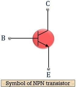
Symbol of NPN:
The following diagram depicts the NPN transistor's symbolic representation:
The direction of current flow through the device is clearly shown by the outward arrow at the emitter terminal in the symbolic representation. Electrons make up the majority of carriers in NPN transistors.
Construction of NPN transistor:
The NPN transistor is built in two ways.
NPN transistors are formed when a p-type semiconductor material (either Silicon or Germanium) is fused between two n-type semiconductor materials, as we already know.
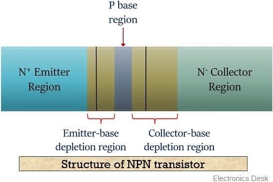
The constructional structure of an NPN transistor is depicted in the diagram below:
The NPN transistor is made up of a number of different components.
It is divided into three sections: emitter, base, and collector.
The emitter-base junction is the region that connects the emitter and the base region. The collector-base junction, on the other hand, is the point where the base and collector regions meet. It functions as two PN junction diodes due to the presence of two junctions in between three regions.
The levels of doping in each of the three regions are different. The emitter region has a lot of doping, while the base region also has a lot of doping. And the collector region's doping level is moderate, falling somewhere between the emitter and the base region. Its inverse is the PNP transistor, which has a P-region sandwiched between two N-Type regions.
It's worth noting that the emitter and collector regions cannot be switched around. The reason for this is that the collector region's thickness is slightly greater than the emitter region. So that more energy can be dissipated.
The NPN transistor's working:
Let's look at how the NPN transistor works now.
When there is no applied bias to the transistor or when there is no battery connected between its terminals. It is then referred to as the transistor's unbiased state. We've already talked about how a PN junction diode works in the absence of bias. A transistor is made up of two PN junctions, as we already know.
As a result, under no biased conditions, electrons in the emitter region begin to move towards the base region due to temperature variations. However, a depletion region forms at the transistor's emitter-base junction after a certain amount of time has passed. Only about 5% of electrons combine with holes in this region after reaching the base region, while the rest drift across the collector region. Similarly, a depletion region forms at the transistor's base-collector junction after a period of time.
It's worth noting that the thickness or thinness of the depletion region is determined by the material's doping concentration. To put it another way, in the case of a lightly doped region, the width of the depletion region will be greater than in the case of a highly doped region. This is why the depletion width at the collector-base junction is wider than at the emitter-base junction. These two depletion regions serve as a potential stumbling block to any further majority carrier flow.
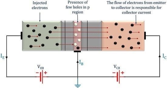
The following diagram depicts the biased condition of an NPN transistor:
The width of the depletion region, also called PN Junction, narrows as a result of the forward applied voltage at the emitter-base junction. Similarly, the width of the collector-base junction is widened by the reverse applied voltage. This is why, in comparison to the collector-base junction in the previous figure, the emitter-base junction has a thin depletion region.
Electrons begin to inject into the emitter region as a result of the forward applied voltage VBE. The electrons in this region have sufficient energy to overcome the emitter-base junction's barrier potential and reach the base region.
The charge carrier movement in an NPN transistor is depicted in the diagram below:
Because the base region is very thin and doped lightly. As a result, only a few electrons combine with the holes once they reach their destination. Because of the strong electrostatic field, electrons begin to drift at the collector region due to the very thin base region and the reverse voltage at the collector-base junction. As a result, these electrons are now collected at the transistor's collector terminal. The electrons begin to move towards the collector as recombined holes and electrons become separated from one another. A very small base current also flows through the device as a result of this movement. This is why the emitter current is equal to the sum of the base and collector currents. IE = IB + IC
Applications of NPN diode:
Transistors with NPN Diodes (NPN) are used in a variety,
- High-frequency applications make use of these.
- Switching applications are where NPN transistors are most commonly used.
- This component is used in amplifying circuits.
- To amplify weak signals, it's used in Darlington pair circuits.
- NPN transistors are used in applications where a current sink is required.
- Some classic amplifier circuits, such as ‘push-pull' amplifier circuits, make use of this component.
- In temperature sensors, for example.
- Applications with extremely high frequency.
- In logarithmic converters, this variable is used.
- Because signal amplification is done with NPN transistors. In amplifying circuits, it is used in this way.
- Logarithmic converters are another area where it is used.
- The switching characteristic of the NPN transistor is one of its most significant advantages. As a result, it's commonly used in switching applications.
NPN transistor terms that are important to know:
Region of the emitter: It is the largest section of the structure, which is larger than the base region but smaller than the collector region. It has a lot of doping in it. It is used to transfer majority carriers into the base region, which are electrons. It is a forward-biased region, which means it is always provided with the base region forward biased.
Region of the base: The base region is located in the middle of the structure. In comparison to the transistor's emitter and collector regions, it has a small region. It is lightly doped to ensure that there is minimal recombination and a high current at the collector.
Region of the collector: It is the structure's rightmost section, and its function is summed up in its name: it collects the carriers transferred by the base region. When compared to the base region, this region receives reverse biassing.
Did you like what you read? Visit your profile and preference center to opt in to our DS newsletter and never miss cool articles again!


Comments