What is MOSFET? A detailed guide on MOSFET
Follow article
 Dave from DesignSpark
How do you feel about this article? Help us to provide better content for you.
Dave from DesignSpark
Thank you! Your feedback has been received.
Dave from DesignSpark
There was a problem submitting your feedback, please try again later.
Dave from DesignSpark
What do you think of this article?
In this post today, I’m going to discuss MOSFETs in detail.
I suggest you read this article all the way through as I’ll cover each and everything related to MOSFETs including MOSFET definition, symbol, working, characteristics, types, and applications.
Definition:
The MOSFET stands for Metal Oxide Semiconductor Field Effect Transistor that is a semiconductor device mainly employed for switching and amplification purposes in electronic devices.
MOSFET is a transistor with four terminals called:
- 1: Drain (D)
- 2: Source (S)
- 3: Gate (G)
- 4: Body (B)
MOSFETs are also known as IGFET (Insulated Gate Field Effect Transistor) as the gate pin is electrically insulated from the semiconductor.
MOSFET is a voltage-controlled device, as opposed to BJT (bipolar junction transistor) that is a current-controlled device.
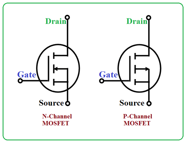
Symbol:
A MOSFET is commonly known as a three-terminal device where the body is considered as the fourth terminal that is internally connected with the source terminal.
The following figure shows the symbols of both N-Channel MOSFET and P-Channel MOSFET.
Working:
The MOSFET is a voltage-controlled device where current flows between drain and source terminal when voltage is applied at the gate terminal. The MOSFET more often operates like a switch and the functionality of this transistor is based on the MOS capacitor which is the key part of MOSFET.
MOS capacitor is a semiconductor surface that lies below the oxide layers between both drain and source terminals.
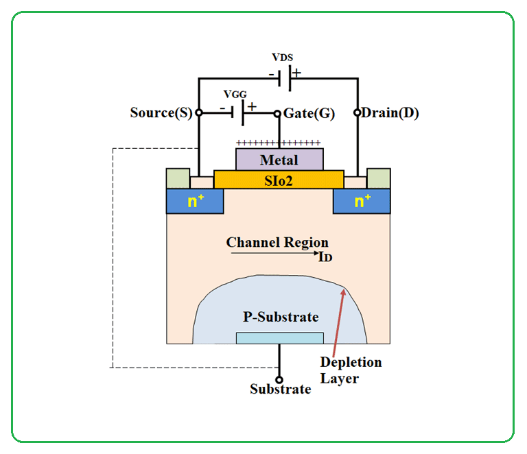
The working of MOSFET is simple and straightforward. In the case of N-Channel MOSFET, when a positive voltage is applied at the gate pin, it produces the conduction process between Drain & Source terminals. In this condition, MOSFET is considered to act in an Enhancement Mode.
The positive voltage at the Gate terminal will attract the electrons below the oxide layer and repel the holes. As a result, the electrons will start accumulating below the silicon oxide layer. The more positive voltage at the gate terminal will attract more electrons and thus conduction process increases in N-Channel MOSFET.
Now if we apply negative voltage at the gate terminal, it will force the N-type MOSFET to repel electrons and attract holes. As a result, there will be no connection between Drain & Source terminals. In this condition, MOSFET stands in the Depletion Mode.
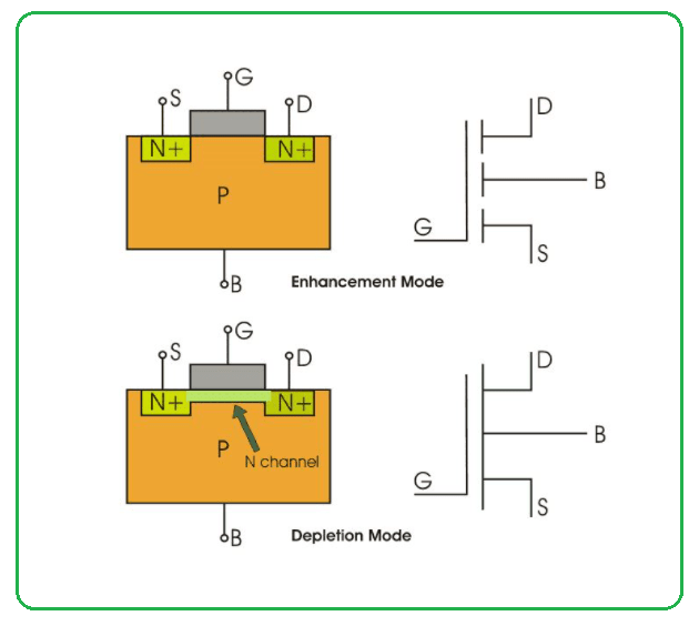
The enhancement mode and depletion mode of MOSFET are shown in the figure below:
Characteristics:
In the enhancement mode of MOSFET, before this device starts conducting, there is a minimum input voltage produced at the gate terminal when gate-source voltage is applied at the gate terminal. This minimum voltage is known as the threshold voltage. To allow these MOSFETs to conduct in the enhancement mode, the threshold voltage must be less than the gate-source voltage.
The forward biasing of MOSFET is directly proportional to the drain current which makes this device a good fit for amplifier circuits. When fixed voltage is applied between the source and drain pins, we can obtain the values of drain current Id at the y-axis for the different values of the voltage applied at the source and gate terminals Vgs at the x-axis as shown below.

The VI characteristics shown above represent the MOSFET transconductance which is a ratio between output drain current and input gate-source voltage.
You can find the transconductance slope by the following formula.
gm= ΔId/ΔVds
Siemens is the SI unit of transconductance and is equal to ampere per volt. Transconductance and voltage gain of this MOSFET is directly proportional to each other i.e. the increase of transconductance would increase the voltage gain.
The graph shown above gives the characteristics curve of the MOSFET. The curve would increase with the increase of drain current as you can see from the figure above that graph turns to linear after it starts as a parabola.
If you want to put the MOSFET in an ON state, the transistor gate should be biased from the given threshold level. And it is important to note that the biasing of gate pin can be obtained with two methods i.e. drain feedback biasing and Zener diode biasing.
Types:
MOSFETs are normally categorized into two types as follow:
- N-Channel MOSFET
- P-Channel MOSFET
Holes and electrons are responsible for the flow of current in these MOSFETs. Let’s discuss the types one by one.
1: N-Channel MOSFET
In N-Channel MOSFET, negatively charged electrons are the majority charge carriers and a single P-layer is sandwiched between two N-layers. This MOSFET carries an N-Channel region that stands between the drain and source terminals. In this type of MOSFET, the body terminal is of P-type while the drain and source terminals, on the other hand, are heavily doped n+ region. When a positive voltage is applied at the gate pin, the current starts to flow between drain and source terminals where the gate terminal controls the flow of electrons.
The following figure presents the structure of N-Channel MOSFET.
2: P-Channel MOSFET
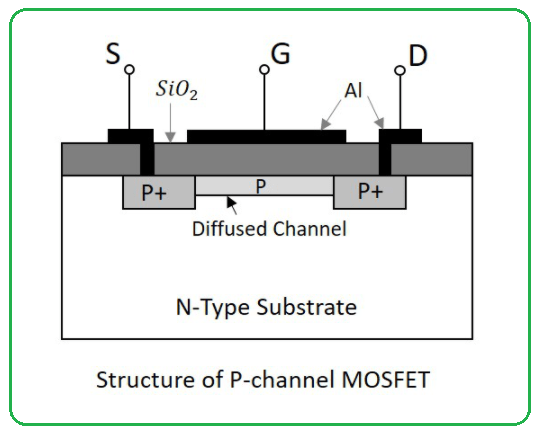
In P-Channel MOSFET, positively charged holes are the majority carriers and a single N-layer stands between two P-layers. This MOSFET carries a P-Channel region that stands between the source and drain terminals. In this type of MOSFET, the body terminal is of n-type while source and drain terminals contain heavily doped p-region. When a negative voltage is applied at the gate pin, the current flows between source and drain terminals and the gate terminal controls the movement of holes.
The following figure shows the structure of P-Channel MOSFETs.
Applications:
- Power MOSFETs are normally employed as switching devices in electronic control units and are widely used in automotive electronics.
- MOSFETs are used in both analog and digital circuits.
- Also used as power converters in modern electric vehicles.
- And in applications where the main goal is to achieve high amplification.
- Mosfets are used in power circuits i.e. Buck Converter or Boost Converter.
That’s all for today. Hope you find this article helpful. If you have any questions, you can approach me in the section below. I’d love to help you the best way I can. Thank you for reading the article.