What is Bipolar Junction Transistor BJT? A Detailed Guide
Follow articleHow do you feel about this article? Help us to provide better content for you.
Thank you! Your feedback has been received.
There was a problem submitting your feedback, please try again later.
What do you think of this article?
In this post today, we’ll discuss BJT (Bipolar Junction Transistor) in detail, including BJT definition, symbol, working, characteristics, types & applications.
Let’s jump right in.
Definition:
The BJT (bipolar junction transistor) is a current-controlled electronic device main employed for amplification and switching purpose. It comes with three terminals called emitter, base, and collector. The small current at the base side is used to control the large current at the remaining terminals. Earlier BJTs were composed of germanium, however, recently silicon is used for the making of BJTs.
Symbol:
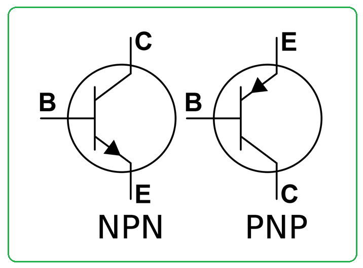
The following figure shows the symbols of BJT. The left one is the symbol of the NPN transistor and the right one is the symbol of the PNP transistor.
The arrows in the symbol show the direction of the current. Current flows from base to emitter in NPN transistor and it flows from emitter to base in PNP transistor.
Working:
The working of BJT starts from the base pin. When voltage is applied at the base terminal in the NPN transistor, it turns ON the transistor and as a result, the current starts to flow from the collector to the emitter terminal. This current is known as the collector current and is denoted by Ic. As this is an NPN transistor, here collector-base junction is reverse-biased and the base-emitter junction is forward-biased.
The depletion region width at the collector-base junction is higher, compared to the depletion region width of the base-emitter junction. The barrier potential is decreased at the BE junction that is forward biased, and as a result, the electrons will move from the emitter to the base region. The base region is lightly doped and is very thin, hence it struggles to hold the number of electrons for the maximum time.
These electrons will combine with the holes present at the base region and start to flow out of the base region as a base current. A large number of leftover electrons at the base region that don’t combine with the holes, then start to enter the collector side, in the form of collector current.
According to Kirchoff’s Current Law, the emitter current is the combination of collector current and base current.
Ie = Ib + Ic
This is the working of NPN transistors. The PNP transistors work in the same way but here current direction and voltage polarities are reversed.
Characteristics:
The BJT is also known as an active semiconductor device where all three terminals are different in terms of doping concentration. The collector side is moderately doped while the emitter terminal is highly doped and the base terminal, on the other hand, is lightly doped.
The BJTs are connected in three different configurations as follow:
- Common-base configuration
- Common-emitter configuration
- Common-collector configuration
Let’s discuss them one by one.
A: Common-base configuration
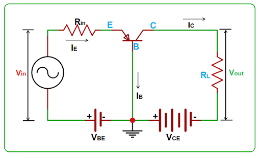
In a Common-base configuration, we will keep the base terminal common between the output and input signals.
The following input characteristic curve for the Common Base configurations is a graph between the emitter current IE on the y-axis and the base-emitter voltage VEB on the x-axis.
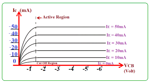
The output characteristics of the Common Base configuration will be drawn between the collector current IC on the y-axis and the collector-base voltage VCB on the x-axis, as shown below.
There are three different regions on the curve named an active region, saturation region, and cutoff region. In the active region, the emitter junction is reverse biased, in the saturation region both collector and emitter junctions are forward biased and in the cutoff region, both collector and emitter junctions are reverse biased.
B: Common-emitter configuration
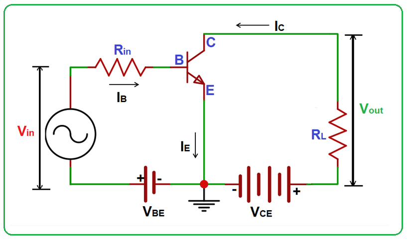
In the Common-emitter configuration, we will keep the emitter terminal common between the output and input signals.
The input characteristics of the Common Emitter configuration is a plot between the base current IB on the y-axis and the base-emitter voltage VBE on the x-axis.
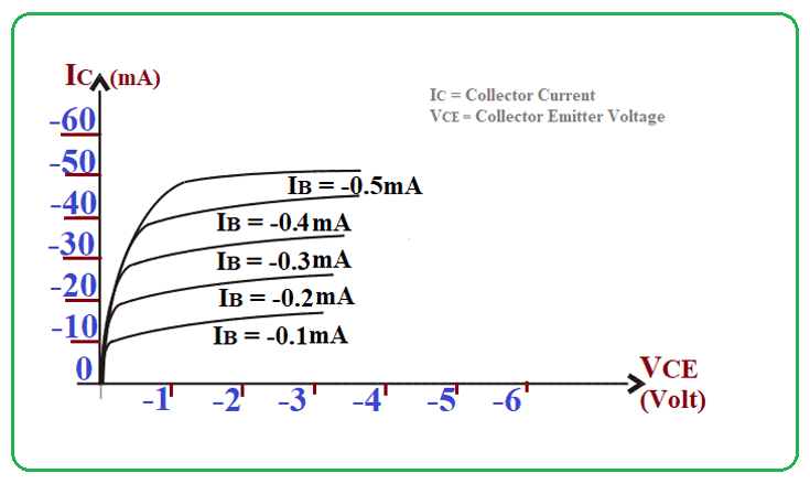
The output characteristics curve is a plot between the collector current IC on the y-axis and collector-emitter voltage VCE on the x-axis. The common-emitter configuration also comes with three regions. In the active region, the emitter junction is forward biased and the collector junction is reverse biased. In the cutoff region, the collector current is not entirely cut off and the emitter junction is not completely reverse biased. In the saturation region, both emitter and collector junctions are forward biased.
C: Common-collector configuration
In a Common-collector configuration, also known as voltage follower circuit, we will keep the collector terminal common between the output and input signals.
This configuration is mainly employed in impedance matching applications and it comes with high input impedance.
Types:
BJT devices are mainly categorized into two main types as follow:
1: NPN Transistor
2: PNP Transistor
Let’s discuss them one by one.
1: NPN Transistor
NPN (negative-positive-negative) is a type of BJT that comes with one P-doped layer that stands between the two N-doped layers. The P-layer represents the base terminal while two N-layers represent the emitter and collector terminals. As this is an NPN transistor, here electrons are the majority carriers and holes are the minority carriers. When voltage is applied at the base terminal, it gets biased and current starts to flow from the collector to the emitter terminal.
2: PNP Transistor
PNP (positive-negative-positive) is a type of BJT that comes with one N-doped layer that is housed between two P-doped layers. The N-layer represents the base terminal while the other two layers represent the emitter and collector terminals. In this PNP transistor, the holes are the majority carriers and electrons are the minority carriers. When voltage is applied at the base terminal, it gets biased and current starts to flow from the emitter to the collector terminal.
It is important to note that the NPN transistors are always preferred over PNP transistors because the movement of electrons is better and more efficient than the movement of holes.
Applications:
BJTs are mainly used for switching and amplification purposes.
BJTs come with low forward drop voltage and better voltage gain, making them a good fit for current, voltage, and audio amplification applications.
Hope you’ve got a clear idea about BJT. If you’ve any doubt about this article, you can approach me in the section below. I’d love to help you the best way I can. Thank you for reading the article.




Comments