Selecting the Ideal ESD Protection Solution
Follow article
 Dave from DesignSpark
How do you feel about this article? Help us to provide better content for you.
Dave from DesignSpark
Thank you! Your feedback has been received.
Dave from DesignSpark
There was a problem submitting your feedback, please try again later.
Dave from DesignSpark
What do you think of this article?
Electrostatic Discharge (ESD) plays a large role in our life, whether we are aware or not. ESD events range from generating charge while walking on carpet and subsequently shocking ourselves on a metal doorknob, to the destructive power of a lightning storm. Many are familiar with ESD protective garments and accessories in a lab environment, but how are our everyday electronics protected from the multitude of possible ESD events?
ESD protection devices protect electronic products from surges and ESD events. Without them, the seemingly harmless shock from touching our laptop could render it useless. To select the ideal ESD protection solution for a given application, we must understand both the system that needs protection, as well as the properties of protection devices. The ESD device must not disturb the functionality of the system it is protecting, and also must react quickly to shunt dangerous current and voltage spikes to ground during surge and ESD events.
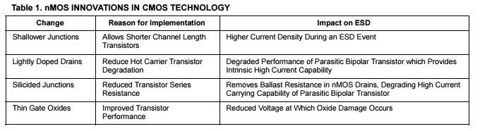
The proliferation of ever-shrinking IC geometries and the fundamental changes that enable these size reductions can have adverse effects on the devices intrinsic ability to survive ESD events. Recent innovations in nMOS transistor technology serve as prime examples of how these changes have degraded the nMOS’s robustness during ESD events.
We'll now take a look at the importance of the various parameters found in ESD protection device datasheets.
DC Parameters
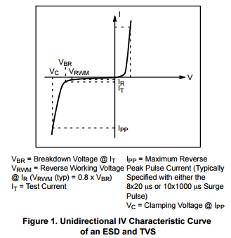
Reverse Working Voltage – VRWM : Maximum nominal working voltage at which the device is intended for use. At this voltage, the ESD diode will appear in the “off” state as a high impedance element that will have very low leakage current.
Forward Voltage – VF : Voltage in the forward direction at the test current IF
Reverse Breakdown Voltage – VBR : At this voltage, the ESD diode starts to conduct, or turn “on”. The breakdown is measured at a test current, IT, typically from 1mA to 10 mA. VBR is specified as a minimum value for ESD applications and usually is 10% to 15% above the VRWM. When selecting an ESD protection diode a designer must ensure that this voltage is higher than the maximum working voltage of the system it is protecting.
Capacitance – C : Capacitance is a parameter that becomes a concern for applications that operate at high data rates. High capacitance will degrade signals, compromising high speed applications. Low capacitance devices are preferred for high speed applications such as HDMI and USB connections.
Survivability Specs
Peak Pulse Current – IPP : Maximum surge current which the device can withstand without damage. This parameter plays an important role to determine the robustness for high power transient voltage suppression (TVS) applications such as inductive switching, but is not as crucial for applications that are predominantly concerned with ESD events such as portables applications.
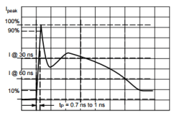
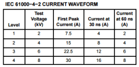
ESD Rating: This is the survivability rating of an ESD protection diode. The most common waveform that is specified is the IEC61000−4−2 system level ESD test which is distinguished by its fast rise time and high current levels (see below). The survivability rating is typically specified by a level or input voltage level per the table below. Most system designers are required to test up to level 4, which is ±8 kV contact or 15 kV air discharge. This rating on an ESD diode datasheet is incomplete, however, since it only tells the designer what the protection diode can survive, but does not give any information as to what voltage level the ESD diode will clamp the ESD pulse to.
Clamping Voltage: In ESD protection applications, the clamping voltage is a crucial parameter that determinesthe voltage that the IC being protected will be exposed to. Since clamping voltage is directly related to the waveform and current level of the surge event being specified it is crucial to examine the conditions of the test for which a clamping voltage is specified. To determine the protection diode with the best clamping performance for an application it is important to look at the clamping performance of the appropriate surge event for that application.
Transient Surge Clamping Voltage: This parameter is a key concern for high power TVS diodes. The clamping voltage is the maximum voltage drop across the TVS diode for a particular peak pulse current, IPP. Since there is no standard IPP or surge waveform for specifying a clamping voltage for ESD protection diodes there is a lot of variance from vendor to vendor.
ESD Clamping Voltage: This property is key for determining the level of protection the protection diode will guarantee against ESD. For sensitive circuit elements it is important to limit the voltage that an IC will be exposed to during an ESD event to as low a voltage as possible. The ESD clamping voltage is the voltage drop across the ESD protection diode during an ESD event per the IEC61000−4−2 waveform. Since the IEC61000−4−2 was written as a pass/fail spec for larger systems such as cell phones or laptop computers it is not clearly defined in the spec how to specify a clamping voltage at the device level. onsemi has developed a way to examine the entire voltage waveform across the ESD protection diode over the time domain of an ESD pulse in the form of an oscilloscope screenshot, which can be found on the datasheets for all ON Semiconductor ESD protection diodes.
onsemi offers a world-class portfolio of ESD protection devices that provide extremely low clamping voltage, low capacitance, and fast response times for applications such as automotive, wireless, and high and low speed data lines.
Discover the ideal solution for your application by viewing the broad portfolio of onsemi ESD devices on offer from RS Components at the link below