Interfacing a 1967 Paper Tape Reader: Part 2
Follow articleHow do you feel about this article? Help us to provide better content for you.
Thank you! Your feedback has been received.
There was a problem submitting your feedback, please try again later.
What do you think of this article?

In Part 1 of this series, I introduced a piece of computing history – data storage on paper-tape – and announced my intention to interface a 1967 vintage paper-tape reader to a modern microcontroller system. I gave various reasons for this seemingly pointless task in that article. Nostalgia is a factor, but I also wanted a vehicle for demonstrating how a product can be engineered for long-term reliability and easily repaired when bits do break. It adds up to what we might call Sustainable Engineering.
The Photosensor Amplifiers
The only electronics built-in to the reader is split between two identical PCBs and consists of nine photosensor amplifiers (a tenth is populated but not used) with a voltage regulator on each board (Fig.1). The boards require a split-rail power supply, which is annoying, but at least it doesn’t have to be precise, with voltages allowed anywhere between ±6 and ±10V. The amplifiers actually work off ±3.3V provided by a simple on-board resistor-zener diode regulator circuit. This regulator also generates the -0.5V bias voltage for the photosensors.

- A single-transistor buffer/gain stage for the photosensor itself, followed by…
- Three transistors that form a Schmitt-trigger to sharpen-up the edges of the pulse waveform making it ‘digital’ in format. This circuit is in turn followed by…
- A single-transistor output buffer that provides a logic signal between 0V and the negative input rail. In other words, the ‘hole detected’ level can be set by the user to be anywhere between -6 and -10V to suit the particular computer hardware. At the time, there were no ‘standard’ logic voltage levels such as ‘TTL’.
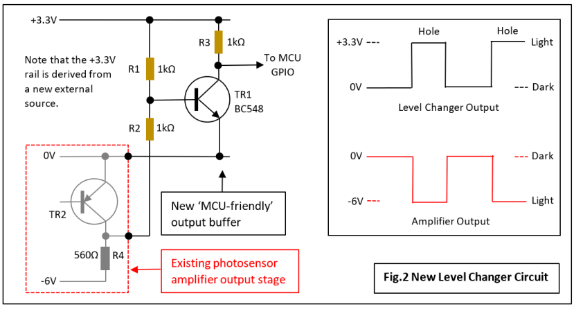
Now a negative voltage is not compatible with modern microcontroller hardware that expects a signal switching between 0 and +3.3/5V. A level changer is required for each of the nine channels (Fig.2).
Output Level Changers
Fortunately, it’s not necessary to track down a suitable chip to perform this task: using the technology of the day, all that’s needed is a general-purpose NPN transistor and three 1kΩ resistors. I chose the BC548 because I happened to have a drawer-full, but a ZTX302 or 2N2222A should work just as well. The circuit is easy to analyse because the signal only has two levels.
Light detected (Hole): TR2 is turned off creating a potential divider with R1, R2 and R4. Hence the voltage on the Base of TR1 is about -0.5V leaving it firmly turned off. The circuit output is nearly +3.3V, being pulled up by R3.
No light detected (No Hole): TR2 is turned on bringing its Collector voltage nearly to 0V and creating a potential divider with R1 and R2 only. The voltage on the Base of TR1 is now about +1.5V, turning it on. The circuit output is thus pulled down to nearly 0V.

As another example of thoughtful design, all nine photosensor amplifier outputs plus the split-rail power supply inputs and ground, are confined to the right-hand 12-pin connector. The 240Vac motor supply, pinch solenoid drive and the heavy-current supply for the lamp are taken to the left-hand 18-pin connector. Run Out and Tape Loaded switch signals also appear here, but no high-speed electronics is involved. This separation helps to minimise the likelihood of data corruption by electrical noise.
Pinch Solenoid Driver
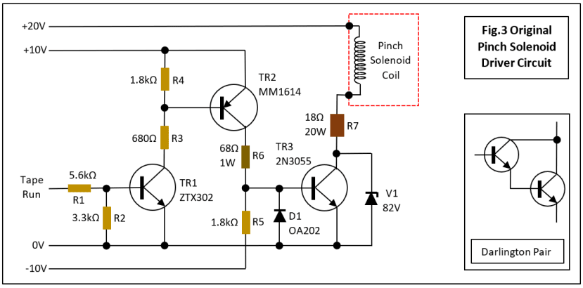
The manufacturer kindly provided a suggested circuit for the solenoid driver in the technical manual for the reader (Fig.3). At first, I thought it would be appropriate to use this ‘recommended circuit’, but this is one instance where nostalgia should give way to a more modern design featuring fewer components.

The only other components of note are the diode D1, an obsolete OA202, but with no shortage of equivalents around, and a Varistor V1. The latter is a Z5D820 over-voltage protection device that’s still manufactured by Semitec, with a direct equivalent ERZV05D820 (720-9740) available from Panasonic. It’s a very important component absorbing the high reverse voltage induced by the inductive solenoid coil when TR3 is turned off. D1 prevents the Base of TR3 being dragged down to -10V when TR2 turns off. All BJTs have a small reverse-voltage tolerance on the Base-Emitter junction and the mighty 2N3055 is no exception with a maximum VEB of only 6V.
An alternative design
There is an extremely useful configuration of two bipolar transistors called a Darlington Pair (see inset in Fig.3). It behaves like a single super-BJT with greatly enhanced performance:
- Increased input impedance and reduced output impedance.
- A gain equal to the product of the individual gains.
The only downside is a doubling of VBE to 1.4V, but the logic input will be at least 3V so that’s no problem. For our purposes, we have a simple circuit that can be driven from a GPIO pin, but itself drive a heavy-current load such as a solenoid or motor. A further big advantage of using a single device is the reduction of three power rails to just one! Naturally, such a useful circuit long ago became available as a single 3-terminal device, such as the one I propose to use here: a BD677A (485-9985) . I’ll report back about how it performs in the next article.
Microcontroller
My plan is for the host computer to communicate with the reader via an RS-232 (UART) serial link. The host will send commands to engage the pinch roller and start the tape moving. The reader will respond with the data, or error codes for conditions such as lamp/motor not powered and tape not present. So, the minimum interface hardware I’ll need is a UART and the best way of getting one of those is to use an embedded microcontroller (MCU) with it built-in. Pins on the MCU will have the following functions:
- 8 x GPIO configured as inputs for the photosensor data channels.
- 1 x GPIO configured as an interrupt input for the photosensor sprocket channel.
- 1 x GPIO configured as an input for the manual Run-Out button.
- 1 x GPIO configured as an input for the Tape Out detection microswitch.
- 1 x GPIO configured as an input for the Lamp/Motor power switch.
- 4 x pins for UART Tx, Rx data and RTS, CTS handshake signals.
There is a huge range of suitable devices, and I’ve not really made up my mind yet. A leading contender is the RP2040 in the form of a Raspberry Pi Pico (212-2162) board. I normally program MCUs in their Assembler language and the ARM Cortex-M0+ code is straightforward, but I’m not sure what tools to use.
Next Time in Part 3
Next time I hope to report a working pinch solenoid controller and a complete set of level changers ready for connection to an MCU. If I can get the components that is – even some small stripboards I ordered are overdue.
If you're stuck for something to do, follow my posts on Twitter. I link to interesting articles on new electronics and related technologies, retweeting posts I spot about robots, space exploration and other issues.

