How Makers, Engineers, and Developers can accelerate development and prototyping with RENESAS RL78/L1A Promotion Board
Follow article
 Dave from DesignSpark
How do you feel about this article? Help us to provide better content for you.
Dave from DesignSpark
Thank you! Your feedback has been received.
Dave from DesignSpark
There was a problem submitting your feedback, please try again later.
Dave from DesignSpark
What do you think of this article?
In the face of increasing competition, and shorter time to market, Engineers and Embedded Developers are under ever increasing time pressure because new product releases need to be available in shorter and shorter intervals. Therefore, they are permanently in quest of flexible, convenient and ready to start development tools that will help them shorten their product development cycles while meeting customer demands and keeping a constant eye on cost.
The first time I got my hands on the RL78/L1A Promotion board I was really impressed! It is a feature-rich rapid prototyping board designed to help engineers, makers and embedded developers to quickly get started and make their new concepts and own ideas a reality without need of additional hardware.
On top of that, makers and developers get the Source Code for Demo application for FREE! Great product, really amazing, it seems and feels way easier than handling similar Development Kits from other MCUs providers. Keep up the good work Renesas!
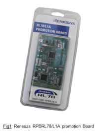
One thing I have noticed while exploring the kit, is that the RPBRL78/L1A promotion board works right out of the box, and comes with all necessary components to make it easy to begin developing and debugging a complete embedded application right away. Figure 2 below shows the complete PCBs set of the RPBRL78/L1A promotion Board that consists of the RL78/L1A MCU board and the Display board.
More details about the RPBRL78/L1A Board and some links where to download the Software and further Documentation of the Kit from can be found at: www.renesas.com/RPB-RL78-L1A
GETTING STARTED WITH RPBRL78/L1A IS EASY!
It is amazing to see how Renesas Electronics has made embedded design with the RL78 microcontroller family as easy as possible.
The board is being delivered pre-programmed with a working and FREE of charge sample demo Software package consisting of signal generator, oscilloscope / data logging application demo which makes it easier for makers, engineers, and developers to quickly get started with the evaluation, accelerate their design and make use of all the possibilities the RL78/L1A device offers right away. The pdf RPBRL78/L1A user manual gives a step-by-step instructions on running the pre-programmed demo, but also, it provides instructions on building working devices that take full advantage of the powerful LCD drive, analog and Low Power features that the RL78/L1A device offers.
Key Components & Features of RPBRL78/L1A
-
24MHz R5F11MPGAFB (RL78/L1A) MCU,
-
128KB Flash, 8KB Data Flash, 5.5KB RAM
-
Integrated E2 Lite Emulator for programming and debugging,
-
integrates seamlessly with e²studio IDE
-
128 x 128 Colour Dot Matrix PMOD Display board,
-
PMOD connector for LCD display board,
-
Header extender for Renesas Standard RSK LCD display board,
-
USB interface (USB-UART serial bridge),
-
Temperature sensor,
-
Various user interface options:
-
Potentiometer for user analogue input,
-
User pushbutton
-
Physical switches
-

MAKE YOUR DESIGN IDEA REAL WITH RENESAS RPBRL78/L1A
-
Application driven approach:
-
Having a rich-featured Evaluation Board with real working Demo application and sample Code examples improves the efficiency of Software development significantly. This is what makes the embedded developers especially happy.
-
-
The RPBRL78/L1A will accelerate the start for your next embedded development.
-
The RPBRL78/L1A comes out of the box with a Programmable Signal Generator and Oscilloscope and Data logger Demo application code
-
The RPBRL78/L1A is designed to showcase the analogue and low power capabilities of the RL78/L1A microcontroller and to provide an easy to use Human-Machine Interface (HMI).
-
The remarkable thing about this is that you can use the provided Demo application code as the base of a real product. All you need is to download for FREE the schematics and 'C' source code that can easily be modified to your specific application needs.
-
-
All features driven by a single device – RL78/L1A - How stuff works ?
As shown in the Fig 3, the analog front end is embedded in the RL78/L1A and utilizes 2x op-amps, a SAR 12-bit ADC, 2x12-bit DACs and configurable voltage reference. The internal RAM is used to store up the working waveform in an absolute buffer. Renesas’s Low Power features like DTC (Data Transfer Controller) and ELC (Event Link Controller) used by the RL78/L1A device help to achieve the low power requirements for this fully integrated Signal Generator and Oscilloscope / Data logger demo.
To illustrate some of the features and benefits of using such a Low Power MCU with rich analog integrated features like the RL78/L1A, let’s closely examine the following Figure 3 which shows the simplified functional block diagram of some of the main features implemented in the RPBRL78/L1A demo application.

Adjustable signal generator
-
A signal generator is derived from an integrated 12-Bit DAC and rail-to-rail operational amplifier, which provides a variety of user-configurable waveforms like triangular, square, sine, etc…)
-
The basic waveform pattern for each waveform type is stored in FLASH memory. However, the working waveform buffer itself is located in RAM memory and is defined by a combination of parameters including the selected waveform pattern, scaling factor and offset values determined by the user in real-time.
-
When a change is made to the any of these parameters by the user, the waveform buffer is recalculated following a predefined algorithm.
-
The timer array unit is then used to schedule the changes to the output at regular intervals defined by the time base of the signal generator
-
Highlight: The signal generator operation is achieved without CPU involvement, reducing its workload.
Programmable gain oscilloscope
-
The oscilloscope section consists of the rail-to-rail op-amp, the 12-bit ADC and the associated analogue and low-resistance switches as well as the display stages.
-
When an oscilloscope trace is not being recorded, the system is waiting for a trigger.
-
The oscilloscope operation uses a DAC channel and the analogue comparator peripheral to trigger the acquisition of an oscilloscope “trace”.
-
Highlight: The oscilloscope trace capture sequence is automatically handled by the ELC and the DTC without CPU intervention
ELC and DTC Event Handling
The RPBRL78/L1A Demo application code demonstrates the use of the DTC and ELC peripherals to perform complex tasks independently of the CPU. This allows the CPU to be doing other things, or to be put into low power modes.
DTC feature: Basically, the Data Transfer Controller DTC allows the transfer of memory from one location to another, based upon hardware events:
-
In this Demo example, the completion of an ADC sample triggers a DTC to append the ADC result to a buffer.
-
The DTC peripheral is also used to update the DAC when the timer interval interrupt occurs so the DAC operation can happen without CPU intervention.
Another DTC feature: DTC operations can also be chained together so a single event can initiate a sequence of operations automatically:
-
In the Demo example, when the comparator interrupt occurs, the DTC starts the first ADC acquisition and then follows a sequence of chained operation directly after this. Finally a separate DTC operation is triggered by the availability of new sample data on the ADC. This DTC automatically appends the new sample to the trace buffer.
-
The acquisition of samples is sequenced by a combination of the DTC and ELC peripherals in the RL78/L1A microcontroller. This reduces the workload on the CPU and facilitates reduced power consumption.
ELC feature: The ELC allows the completion of an operation of a peripheral to trigger the start of another one:
-
Highlight: The ELC is configured to start an ADC conversion automatically each time the timer interval interrupt occurs. This implements the regular acquisition of data from the oscilloscope allowing the ADC conversion to happen independently of the CPU. This allows the CPU to be doing other things, or to be put into low power modes to save power.
Human Machine Interface
-
The application provides a simple to use menu system for the user to configure and operate the oscilloscope demonstration.
-
the resulted voltage waveform is displayed in real-time by the oscilloscope
-
- output either to on the PMODTM via the SPI interface
- or output on the Virtual COM Port via the UART interface
Software & further documentation for this Renesas kit is available for download from: www.renesas.com/RPB-RL78-L1A
Inquiries:
https://www.renesas.com/en-eu/support/contact.html
Technical Contact Details:
https://www.renesas.com/en-eu/solutions/key-technology/human-interface/rl78-l1a.html
Website:
Europe: https://www.renesas.com/en-eu/support/contact.html
Website: http://www.renesas.com
Comments