Ground loops and other pitfalls in shop floor communication
Follow article
 Dave from DesignSpark
How do you feel about this article? Help us to provide better content for you.
Dave from DesignSpark
Thank you! Your feedback has been received.
Dave from DesignSpark
There was a problem submitting your feedback, please try again later.
Dave from DesignSpark
What do you think of this article?
You can find tons of excellent articles about ground loops on the internet. This article is not another general introduction to this topic. Instead, I want to focus on two specific real-world problems: Digital communication lines in factory automation on shop floors (so-called “field busses”) and the pitfalls of using the USB in such environments.
Field Busses
Many wired serial busses used in manufacturing automation are based on EIA 485 or Ethernet definitions. The physical layer of Ethernet has integrated galvanic isolation (so-called “magnetics”), and thus the signal potentials are ground-level-independent to a great extend (up to several kV). So I will focus on the EIA485 based field busses: Modbus RTU, Profibus DP, Bitbus (IEEE 1118), DMX (stage technology), and so on.
Ground-level dependency
Most engineers know EIA485 as a “differential” bus and thus conclude that it is ground-level-independent. A short glance at a typical physical level interface (bus transceiver) does show you that this is a common misunderstanding.

The logical level is defined by the voltage difference of A(-) and B(+) terminals. But both, the driver and the receiver refer the A and B voltages to their local GND potential. The mean value of the A and B voltages is called common-mode voltage (VCM). The EIA 485 definition limits the common-mode voltage to -7 V to 12 V. Voilá; we have the ground-level dependency! Imagine the driving circuit references to its local GND, and this potential is 30 V away from the receiver’s circuit GND potential.
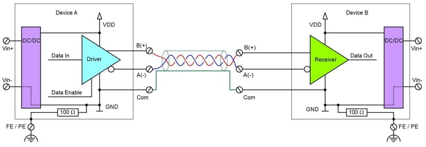
So without any galvanic isolation, we need similar GND potentials for driver and receiver. One approach to this goal is a third line connecting the driver’s GND with the receiver’s GND (often called “common line”.

Profibus DP is consequently going this way, and other technologies (DMX, Modbus RTU) strongly recommend using an additional GND (“common”) connection. However, many engineers with substantial practical experience don’t like GND connections in EIA 485 lines. They are convinced that disconnecting the GND connection at one end of the cable shield often solves problems with poor transmission quality.
Controversies about the mystical third wire
So why is there a difference between theory and practical experience? The answer is “ground loops”.

Let’s get back to our example: There is a potential difference of 12 V between the two GND levels. The EIA485 receiver would barely tolerate the 12 V common-mode voltage and deliver an error-free signal. Now we are connecting the two GNDs using the cable shield. This results in a potential high current flowing over the shield. The shield is part of a ground loop. We get in big EMI trouble if the 12 V GND differences are AC transients (a typical industrial shop floor situation). The shield is a perfect capacitive coupling device for the A and B signal lines. While the common-mode voltage is forced to a near 0 V level, it becomes an uncontrolled unbalanced EMI signal on our signal lines, much higher than the +/- 2 V signal level.
EIA 485 suggests lowering the shield current by adding 100 Ohm resistors between each device’s signal GND and earth potential. Most of the common-mode voltage will then drop over these resistors.
Functional Earth: The magic wand for an equal reference potential
Profibus DP explicitly demands additional low impedance grounding of each device to minimise shield currents. High-quality industrial devices always have additional “functional earth” (FE) connectors (sometimes screws) for separate one point grounding. Their internal (signal) GND path is separated from this functional earth by HF filtering and other protective elements. This is a primary way to keep high energy EMI (surges, bursts) away from internal signal GND and supply voltages. The current loop for EMI signals flows through the power supply lines, blocked to pass into the device and forced back through the protective components over the FE-line. With such devices and correct FE coupled GND potentials, you will get fewer problems when establishing a low impedance “common”-line (at signal GND level).
Bus-powered devices: The solution for process automation
Profibus PA and Foundation Fieldbus (FF H1) both choose another approach to avoid ground loops. Their purpose is to connect remote field devices (like valves or sensors to a control system in a process automation environment. The control system uses the two differential bus wires also to power the remote devices. This ensures equal GND potentials on both ends as long as the remote devices’ signal GND is not connected to FE or PE. With these busses, the shield needs always to be unconnected at the remote end and connected to FE at the control system. With such a configuration, you can safely transmit digital signals over several kilometres.

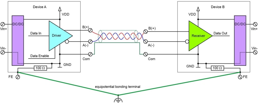
Galvanic separation: Best choice for all situations
Of course, the gold standard to avoid ground loops is a galvanic separation between the bus wires and the electronic circuits sending or receiving the bus information. Such systems will always need the isolation of the bus signals (optical, capacitive or magnetic coupling) and an isolated power supply for the signal line drivers. As there is no FE or PE connection of the bus, you might think there is no common-mode voltage. But the drivers can switch to the idle state (high impedance), and the receiver’s impedance is also very high. EMI could load even the most minor stray capacities to several volt common-mode. So it is wise not to leave the bus floating at nowhere but to tie both ends to the same internal signal GND by using an additional third wire. As the equilibrating currents are minimal, we can safely use the shield for this purpose. But you need to be aware that your galvanic separation must handle the offset potentials between both sides of the separation (the non-isolated part of the device will probably have its signal GND connected to FE/PE).

Reference design from Maxim's application note 2116 typically (189-9578)
USB in industrial automation
EU directive 2004/108/EC defines electromagnetic compatibility as the ability for a device to function acceptably in its specific electromagnetic environment. This includes a limitation of EMI emission as well as a susceptibility for existing EMI. The directive does not define certain limits but refers to individual normative rules to regulate such limits. The EN 61000-6 is such a norm. It defines the limits for emission and susceptibility for specific environments (part 2 and 4 for industrial environment, part 1 and 3 for consumer products).
While the demands for consumer products focus on low emission, the demands for the industrial environment focus on high EMI susceptibility.
This results in problems when using typical consumer technology in an industrial environment. Engineers who integrated USB into industrial automation equipment know about the problems I’m talking about. USB cable length is often limited to small values in the conformity declaration to achieve the demanded EMI susceptibility. This trick facilitates omitting the EMC tests for “conducted disturbances”, which are frequently not passed by typical USB components.
The hidden short circuit
One major problem with USB is how many USB devices handle USB power and shield provided by a USB host. As stated earlier, a typical industrial controller would distinguish between the cable shield (typically connected to FE) and the V-bus (5 V) GND potential. The latter per definition is the reference potential for the differential USB bus signals. However, most consumer USB devices like memory sticks or Wifi/Bluetooth transceivers do not make this distinction. Instead, they connect the shield to the V-bus GND line. When I constructed the Revolution Pi controller, I was not aware of this problem. I hardened the power supply electronics to withstand all the tortures of industrial compliance tests. Out-of-range or reverse connected 24 V, GND, and FE wiring was no problem in all demanded test situations. But these tests have been made without any USB wireless dongle or memory stick inserted into the USB ports. But then we had device returns from customers who burned their RevPi by accidentally confusing the FE and +24 V input terminals. We found out that they all had USB devices inserted. And here is what happened:


Schematics from the only open-source industrial controller Revolution Pi typically (182-5570)
The USB device shortened FE and internal RevPi GND. This established a ground loop. By swapping +24 V and FE, they ended up with 24 V between external GND and internal GND. However, too much current for the protective components separating internal GND from external GND caused some smoky puffs and killed the common mode choke.
Even if the users would not mix up 24 V and FE connections, we end up with several protective elements of our device to be shortened by a plugged-in USB device. Moreover, the direct connection of the USB shield with internal GND opens a pathway for all kind of EMI to pollute our internal GND potential.
Inserting a resistor between the USB shield and FE would not help either. However, it would eliminate the risk of high currents resulting from confused power supply connections. But it would keep out EMI from our internal GND.
Using a galvanic isolated DC-DC supply section (external 24 V to internal voltages) seems to be an excellent idea to eliminate most EMC problems. But exposing the internal GND to any external cables or devices would always risk the integrity of the internal signal GND potential.
The only way out is an expensive and bulky provision of galvanic separated V-bus for the USB host connectors. Such a DC-DC device would need to deliver at least 2.5 W per port (even more for USB 3). But it provides another GND potential that can be a reference for the USB signals and is used as V-bus GND. Thus, any connected device powered by V-bus may shorten the shield and V-bus GND with minimal consequences for the signal integrity and none for the USB host electronics. Here is an integrated solution from Analog Devices, the LTM2884: typically (760-3312)

Picture from the LMT2884 product documentation
Swarm Experience
I hope this practical example could demonstrate the complexity of ground loops in industrial communication. At the end of the day, our designs all have to pass compliance tests and the field experiment of satisfying our customers with all their unique environments. This makes perfect ground concepts a topic where theory is essential, but the experience is even more. DesignSpark wants to be a platform where we can exchange our experiences. There is not only “swarm-intelligence” but also “swarm-experience”. So why not share your experiences, failures and successes on DesignSpark? We all can learn from it!