DSPCB Engineer - A walk through the many "Settings" Part 1
Follow article
 Dave from DesignSpark
How do you feel about this article? Help us to provide better content for you.
Dave from DesignSpark
Thank you! Your feedback has been received.
Dave from DesignSpark
There was a problem submitting your feedback, please try again later.
Dave from DesignSpark
What do you think of this article?
Note: this article is relevant to users of DesignSpark PCB with an Engineer subscription or looking for more information before upgrading.
As DSPCB Engineer has many advanced features it also has many more settings than DSPCB Explorer, here we provide a quick tour to help you identify some of the key ones that will be of interest.
The settings are available from the menubar <Settings> - <Preferences> and as you will see these are organised in groups under nine tabs.
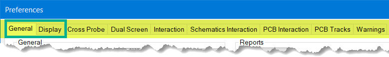
The following is part 1 of the tour and covers the "General" and "Display" tabs.
General Tab.
Design Backups provide an important feature to reduce the possibility of losing your work. This can be configured for the number of backups, their location and with control over their frequency.
An article is available here.

You will also notice two options under the Design Backups option, "work time" and "idle time", and how they further enhance the backup tool can be found in the built-in software help.
<Help> <Online Manuals> <Update Notes>
Most of the other options on the General tab are self-explanatory, and further information if required is available in Help.
Display Tab.
As with many of the tabs, this has many options, but some we would like to bring to your attention are highlighted in the "Drawing" section.
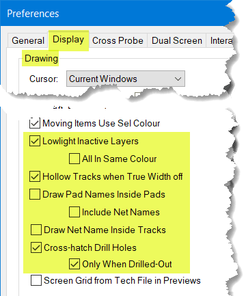
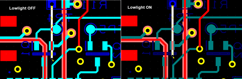
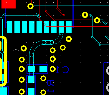
Lowlight Inactive Layers is a great feature when routing your PCB, only the active layer that you are routing on is shown at normal brightness making the working layer the focus of the task. Other layers are 'lowlighted' such that they are still visible to aid the route positioning to avoid signal-coupling etc. Illustrated below is a simple double-sided PCB, this feature is even more valuable with 4 or more layers.
Here' a short GIF demo:

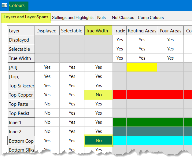
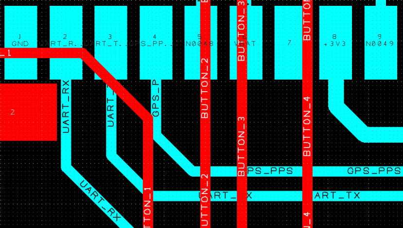
Hollow Tracks when True Width off.
This can initially cause some confusion when looking for the "True Width" setting to turn it on and off!
True Width is a setting by layer, so this setting is in the Colours menu/window as shown below for the top and bottom layers.
With True Width, "Off", and "Hollow Tracks..." selected the PCB view is as below. This can provide a useful clear view to assist in the layout with each segment visible.
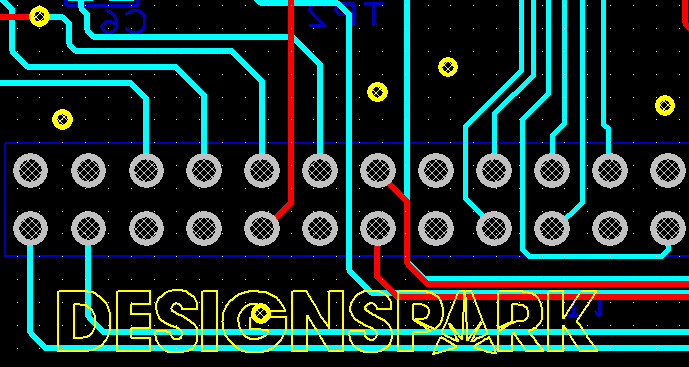
Including pad names in pads or tracks.
These options provide the net or pad names permanently present rather than temporary with the 'mouse over' display.
Cross-hatch drill holes.
This is particularly useful for displaying mounting holes when 'drilled-out', i.e. the hole size removes all of the copper pad area.
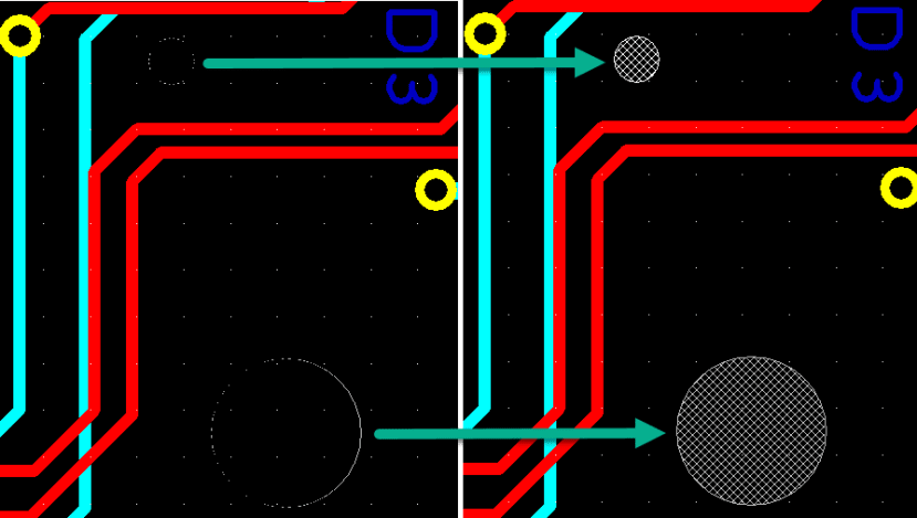
You can also use cross-hatched holes for all holes if you prefer.
Looking at some further options on the Display Tab.
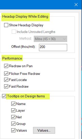
Headup Display While Editing.
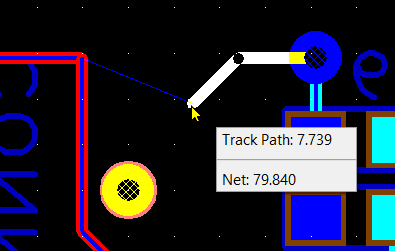
This allows real-time track length information to be displayed.
The top "Track Path" shows the track length from the start point to the endpoint if the net line (blue) is followed.
The "Net" value shows the total length of tracks on that net including the above track that is being placed.
Performance.
These options let you match DSPCB Engineer for the best performance on your Windows system.
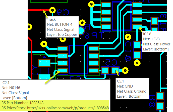
Tooltips are configurable to display items you require.
The "Values" option can be further configured as shown for IC2.
If you haven't yet upgraded to Engineer, the following show the full settings options for the "General" and "Display" tabs.


Part 2 of the tour will cover the "Cross Probe", "Dual Screen" and "Warning" tabs.