DSPCB - Pad Style Exceptions used to produce fiducials.
Follow article
 Dave from DesignSpark
How do you feel about this article? Help us to provide better content for you.
Dave from DesignSpark
Thank you! Your feedback has been received.
Dave from DesignSpark
There was a problem submitting your feedback, please try again later.
Dave from DesignSpark
What do you think of this article?
Note: to use the below features, you will need DesignSpark PCB with an Engineer subscription.
With an Engineer subscription, DSPCB provides a significant advantage over the free software in allowing independent control of the solder/resist mask and the paste mask. This feature allows the custom generation of for example fiducials.
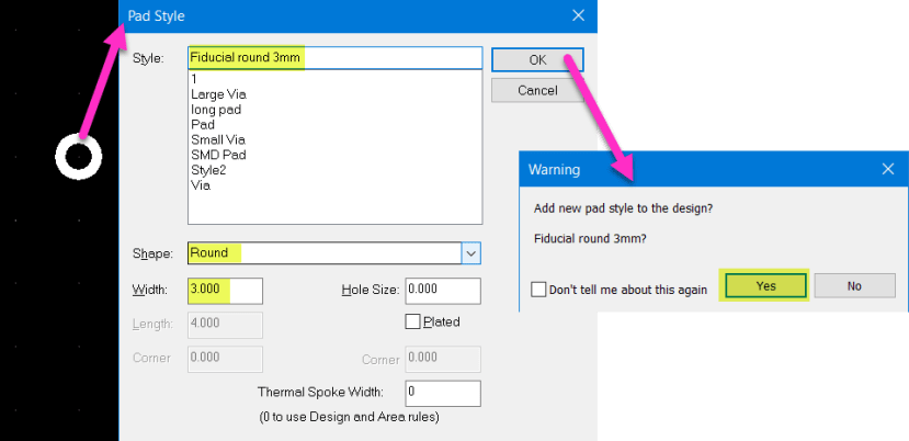
First select "Add Pad" and use the shortcut "S" to change the style, here we set it as a 3mm copper pad and name the style as required and add it to the Design Technology.
For a view of the copper, solder mask and paste mask showing all at once, change the Layers order in the Design Technology as shown for the Paste Mask: Top Copper: Top Solder Mask.
Select the pad and change the layers from "All" to "Top".
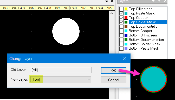
You can now see the opening in the Paste mask and the Solder Mask in relation to the copper pad size.
Now we show how to use the Pad Style Exceptions to customise the Solder Mask opening and remove the Paste Mask opening for a fiducial.
Launch the Design Technology - shortcut Shift+T and select the "Pads Style" tab.
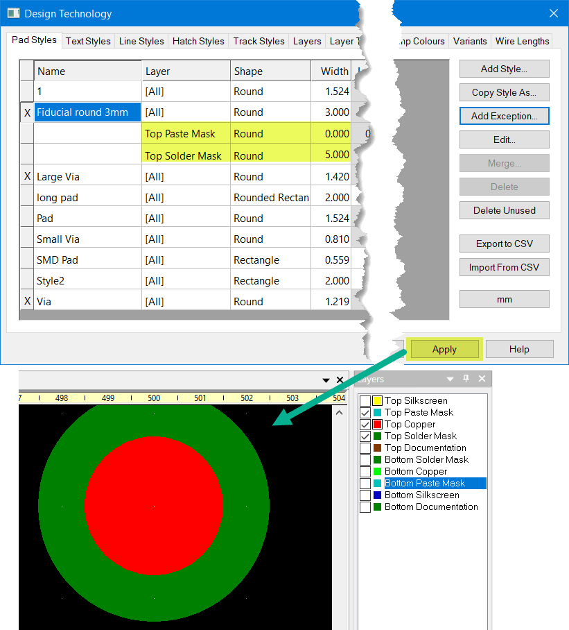
Here you will see our new Fiducial in the list, select it and click <Add Exception> which opens the new Pad Style Exception window, select the Layer "Top Solder Mask" and enter a width of 5.0 and click <OK>, this will create a new entry.

Repeat for the Top Paste Mask and set the width to zero, i.e. no opening in the paste mask.

You will now see the two new entries.
Note they do not have an entry in the "Name" column which indicates they are part of the "Fiducial round 3mm" pad above.
Click <Apply> and you will see the pad in the PCB editor update with the new values, i.e. the larger Solder Mask opening and no Paste Mask.
At this point you have the exceptions applied to the top Solder and Paste Masks, however, if you were to change the layer of the pad the openings are still set at the default values for the bottom layer, so repeat the exceptions for the bottom layer in the Design Technology.
You will now have the Pad Style Exceptions complete. As mentioned the four exceptions are for the part of the above-named Pad Style.

All pads are assigned to [All] layers in the Design Technology, the actual layer [Top] or [Bottom] will be applied in the PCB Editor window when creating a fiducial component. This process is discussed here in this article.
If you are creating a pad style with exceptions for a more general pad than a fiducial and you will reuse it, you may wish to save the pad style in the Design Technology.
Below illustrates the easiest way method and ensures you do not add any unintentional features.
For convenience, it is however illustrated with the above fiducial pad style. To ensure only new "Pad Style" created is saved to the Design Technology in the PCB design editor delete everything in the view.
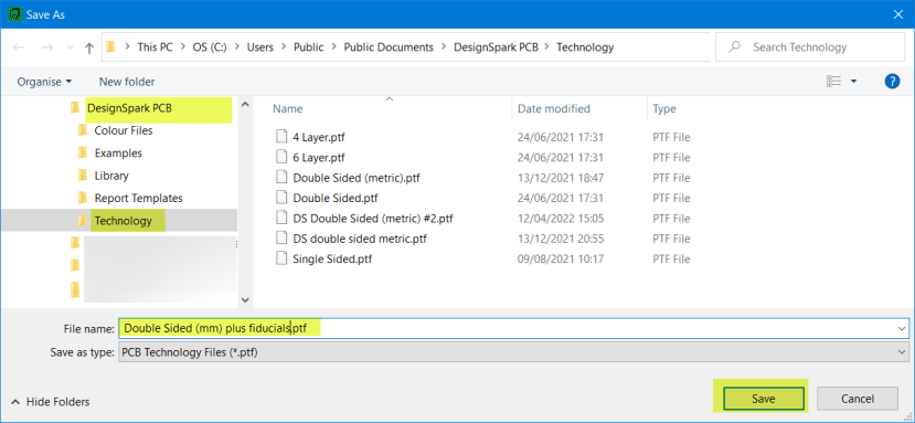
Now from the menubar select File - Save Technology File.

A new window opens where you can enter a new technology file name to avoid any risk of overwriting the original.
Below we show an appropriate name and click <Save>.
The new technology file is now ready to use in all new projects.
When creating a new design using the PCB Wizard simply select the new Technology file.

When you have completed the steps in the Wizard you will see the new Fiducial Pad Style in the Design Technology ready to use in your new design.

As mentioned, the pads are [All] layers, so when a new pad is added, simply select and use the shortcut "L" to change the layer to [Top] or [Bottom] as required.
Using the above Fiducial Pad Style we can also create a PCB only component.
As mentioned you do not have to save this fiducial example in the design technology and can go straight to the steps of producing a component.