Cypress’ NOR Flash memory solution for fail-safe 5G Network
Follow article Dave from DesignSpark
How do you feel about this article? Help us to provide better content for you.
Dave from DesignSpark
Thank you! Your feedback has been received.
Dave from DesignSpark
There was a problem submitting your feedback, please try again later.
Dave from DesignSpark
What do you think of this article?
The next generation of mobile internet connection is almost here. With much faster transmission speed and lower latency, the 5G will reshape our lives. Apart from being able to download high definition movies on your phone in minutes, the implementation of 5G networks will provide much needed extra bandwidth for Internet of Things (IoT) applications.
The 5G connectivity is an integral part of data-intensive applications in industrial settings such as predictive maintenance and robotics control. Near real-time communication achieved with the 5G network also enables the range of applications that were thought to be impossible before. Autonomous driving is an example of how improved latency of 5G opens new technological opportunities to us.
Along with high bandwidth and low latency, reliability and safety are the primary concerns for industrial and automotive systems. The newest high performance, safe and reliable Semper™ NOR Flash memory (197-6854) family from Cypress is compliant with both ISO26262 safety standard for automotive systems and IEC 61508 safety standard for industrial control systems. The family provides superior endurance of up to 1+ million program/erase cycles and data retention of 25 years at extreme temperatures (-40° C to +125° C).
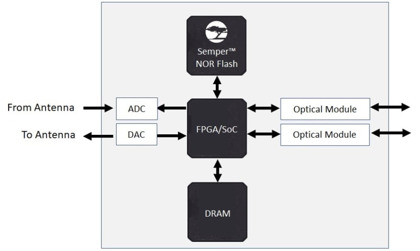
How NOR Flash memory is used in 5G wireless infrastructure
Field-programmable gate arrays (FPGAs) and system-on-chip (SOCs) that are common in cellular infrastructure need to be configured each time they are powered up. External memory devices such as NAND Flash and SD cards can be used for that purpose. Unlike its competitors, Semper NOR Flash memories offer density from 256Mb to 4G satisfying the high bandwidth requirements of 5G technology. Higher density means the memory has more logic elements allowing to process the data arriving/leaving at very high speed (up to 10 Gb/s). Semper NOR Flash devices are compatible with Xilinx, Intel/Altera FPGAs and SOCs from NXP, Renesas and TI.
Key features of Semper NOR Flash memory
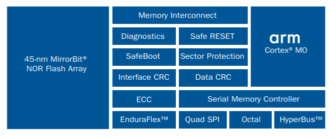
- 45-nm MirrorBit (2-bits/cell) technology supports high-density scaling
- Error Correction Code (ECC), consisting of Single Error Correction and Double Error Detection (SECDED), is generated during memory array programming
- Data Cyclic Redundancy Check (CRC) is performed during system boot or per user command
- Interface CRC is performed to detect accidental faults during data transmission between the host and memory
- SafeBoot ensures bootup failure recovery by reporting the status
- Safe Reset feature can initiate SPI flash hardware reset when the device stops responding to the host
- EnduraFlex architecture optimizes high endurance and long retention of flash memory
- JEDEC xSPI-compliant Quad SPI, HyperBus, and Octal interfaces
Functional safety features of Semper NOR Flash memory are described in more detail in the video below.
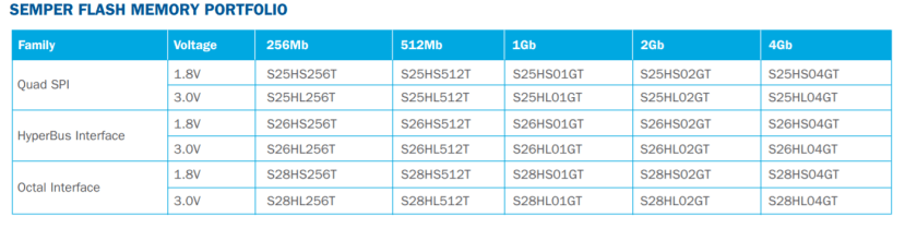
Semper NOR Flash Memory Portfolio
The table below demonstrates the NOR Flash memory portfolio. The family supports Quad-SPI (4-bit), Octal-SPI (8-bit) and HyperBus (8-bit) interfaces. As compared to parallel interfaces, the use of the Quad-SPI interface on NOR Flash devices allows reducing the pin account, hence facilitate the reduction of PCB size. The performance of Octal-SPI and HyperBus can reach up to 400 MB/s.