Introduction to FPGA Programming
Follow articleHow do you feel about this article? Help us to provide better content for you.
Thank you! Your feedback has been received.
There was a problem submitting your feedback, please try again later.
What do you think of this article?
Learning Verilog basics and driving a paper tape punch at Chip Hack EDSAC Challenge
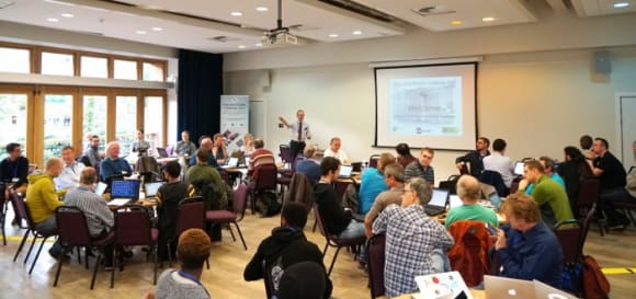
Chip Hack EDSAC Challenge ran as part of the 2017 Wuthering Bytes festival. Hosted by the BCS Open Source Specialist Group (BCS OSSG) and Computer Conservation Society (CCS), and produced by Embecosm, the event aimed to provide a gentle introduction to the world of FPGAs and Hardware Description Language (HDL), in this case Verilog.
Similar events had been run before, but a few key things have come together to make this year, if not the most interesting, certainly filled with historical insights. One of the many more interesting points was that the whole event was based around using a new open source FPGA toolchain.
EDSAC
In a previous article we went into the background of EDSAC. If you missed this, EDSAC was a very early and prominent computer in the earliest days of computing. The CCS and The National Museum of Computing are in the process of producing a full size replica of EDSAC running on the same hardware as the original machine. This is nearing completion and within a short time you will be able to not only visit, but run code upon it.
Hardware Descriptive Language
HDL is not generally a term heard outside of a few niche circles. However, it has a significant effect on our day-to-day lives. From your smart phone, PC, watch and even toothbrush (if you have an electric one), the devices inside will be designed with HDL. Almost every IC in the world will have some form of HDL in their history.
There are two main variants of HDL, VHDL and Verilog. That is not to say there are not any others, but just like software some languages are more pervasive than others. Also just like software some languages are better at some things than others. While Verilog tends to be preferred for chip design and VHDL for FPGA work, this is not mutually exclusive and both languages work for both fields. An analogy would be picking between Java and C++.
For the Chip Hack event Verilog was the language of choice — it is a little more C-like than VHDL, so can be better for those who have not used a HDL before.
Silicon design is out of scope
While HDL can be quick to code, the process of turning this into physical hardware is rather complicated. So much so there are only a handful of silicon foundries or “fabs” in the world. The process of producing wafers and then finally chips, is eye-wateringly expensive — even on the older technology. Most fabs are set up for very high volume throughput, producing millions of wafers and eventually chips per day/week. So how do we test out the Verilog we write?
Introducing the Field Programmable Gate Array (FPGA). While a relatively old technology, having been around since the mid 80s, FPGAs have had limited traction outside of certain applications. This has been due to a few reasons, but a major factor has been the cost. Up until recently they were expensive — so disproportionate to the ASIC that they could not be considered for commercial electronics.
This is changing and there is a very distinctive move to more cost effective parts, and there are a few devices who have chosen FPGA for major roles in their designs. An example is the HTC Vive VR headset, using the FPGAs to fulfil a role not provided by traditional ASICs. A second example is the mobile markets using FPGA for DSP functions; while software can do the same job it requires significantly more power than the FPGA would to achieve the same task; examples for this would include voice recognition. Most of the major players in the FPGA industry have started producing “small” FPGAs to fill these roles. It turns out “small” is not small at all and EDSAC would easily fit in the smallest of these devices.
MyStorm — iCE40
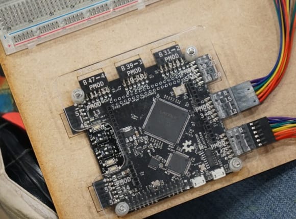
myStorm is the recent creation of Alan Wood and Ken Boak, an open source Lattice iCE40 based FPGA design. The catalyst for this design coming to fruition was the Project IceStorm from Clifford Wolf, the missing link in providing the first ever fully open source FPGA flow. Between this and the cost effective FPGAs appearing on the market, project myStorm was born.
A gentle start
Starting a new language can be extremely daunting, however most software languages follow the same theme; software typically is run in a linear fashion and concurrent code is not the norm. Even if we take the step to concurrent code by using threads, it is fairly explicit that we are doing this. Once we are finally running concurrent code threads, within a single CPU these are run one-by-one and not in parallel. This is changing as we get to multi-core systems, but truly parallel computing is abstracted so far from most software that we need not worry.
This is not the case with HDL and while Verilog looks like C, what we are describing is digital circuits and these do not run one by one — they run in parallel. In fact getting systems to run sequentially requires special attention as this is not the norm for hardware.
To this extent a good proportion of the first day was spent getting the most simple of designs to work and methods to use the hardware effectively.
We all have to start somewhere, so getting an LED to light up is a good start and this was example 1. The chip configuration was provided with human readable names, leaving a single Verilog file:
module led (output led);
	assign led =1;
endmodule
Wow, simple!
Things quickly escalated from making “led = button;” to blinking the led(s).
module blink(input clk, output led);
	reg [24:0] count;
	assign led = count[24];

	always @(posedge clk)
	    count <= count + 1;

endmodule
At this point we had switched from combinatorial logic to sequential, and from blocking to non-blocking assignments. A key distinction that we needed to get to understand in detail.
Combinatorial logic
When we imagine a logic circuit, we most often imagine combinatorial logic. An example would be the circuit below. The AND will immediately reflect the changes on the inputs of the XOR and NOT gates. I.e. parallel tasks.
Sequential logic
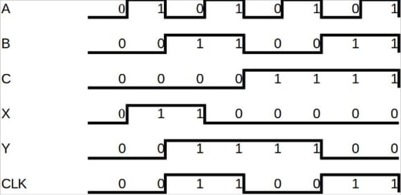
To make the circuit above sequential we need to gate the signals. By using a D-type flip flop on the output we can drastically alter the behaviour of the circuit. In this example we would latch the output and synchronise it to our internal clock.
As can be seen above, if we have a clocked IC by using sequential logic we may miss the output “X”. However, by using sequential logic we retain X’s state until we are ready (state “Y”).
Blocking vs. non-blocking
While a little more difficult to explain we’ll give it a go using code. We have n which is out, input we wish to store n-1 (n1) and then clock out y.
always @(posedge clk)
begin
	n1 = n;
	y = n1;
end
As n changes so does n1. Therefore in effect n = n1 at all times. We also have no control over when n1 finally takes n (which could be a complex combinatorial logic block). The effect being y=n.
Lets change to non-blocking assignment:
always @(posedge clk)
begin
	n1 <= n;
	y <= n1;
end
Now n will get assigned to n1 still, but only at the clock positive edge. y will also take the state of n1, but this time at the same point in time of the posedge of the clock. Therefore y is n-1 not n!
Original works
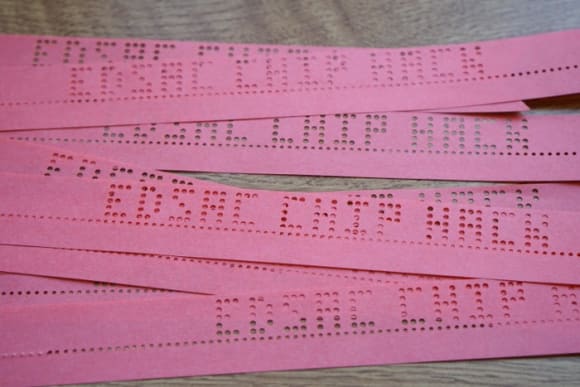
As the event progressed we quickly picked up the skills required to get the EDSAC example running (mostly). While an amazing achievement, as with anything, using provided code is just not the same as creating original works. So at this point we were turned loose to create anything we wished. Not wanting to waste the effort on the PSoC powered tape punch we decided to create a legible header souvenir for the event. If you have read the previous article you may have noticed the header photographed within.
After an initial attempt to create a triple nested state machine design was met with limited success, we (many thanks to Embecosm for the idea) decided it may be simpler to create the data stream and rotate the data out directly from a single register.
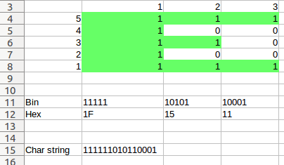
The punch we are using is configured for 5 Bit data with a clock, creating a legible pattern is quite simple using a spreadsheet.
From here it was a case of building a data steam 465 bits long (93 chars long) and prefix it with 465’b, which means 465 binary bits and tells Verilog how to store the data:
465'b000000000000000000000000000000000000000000000000000000000000000000000000000000000000000000000001111110101100010000011111100010111000000110011010110011000001111110100111110000011111100011000100000000000000011111100011000100000111110010011111000001000111111100010000011111101001110000000000000000011111001001111100000111111010011111000001111110001100010000011111001101101100000000000000000000000000000000000000000000000000000000000000000000000000000000000000000000000;If we have the following code we can load “out”, which is assigned to the correct pins on the punch, with the data from our giant shift register.
out <= data[464:460];  // output the top 5 bits of data
data <= data << 5; // shift the data for next time
Next we need a state machine to control the operation states will need to be:
- Idle/ do nothing / reload
- Punch assert data
- De assert data and punch
This equated to a 4-state state machine:
// The state machine
// 0 - initial state
//     action: get the next 5-bits
//     goto state 1
// 1 - assert punch
//     goto state 2
// 2 - deassert punch and initiate punching until done
//     if not done goto state 0
//     if done goto state 3
// 3 - idle state
//     goto state 3
reg [1:0] state = 3;
After much coding and a little experimentation, we eventually ended up with the following code, which once loaded onto the FPGA had us punching legible headers to our hearts content:
module punch(input clk, input reset ,input but0, output led,output led2,output led3, output led4, output D8, output D7, output D6, output D5, output D4, output pclk);


	reg slowclk;
	reg [4:0] out; // register to hold output
	// reg punch; // punch control not used
	reg [7:0] charcount;  // Number of 5-bit char blocks. Enough for up to 256 chars (this would include lead in and out)

	// The state machine
	// 0 - initial state
	//     action: get the next 5-bits
	//     goto state 1
	// 1 - assert punch
	//     goto state 2
	// 2 – de assert punch
	//     goto state 0
	// 3 - idle state
	//     goto state 3
	reg [1:0] state = 3;

	// The data to punch
	reg [464:0] data;

	assign {D8,D7,D6,D5,D4} = {out}; // map the output pins to the data

  	reg [21:0] count; // register to hold clock counter
	assign slowclk = count[21]; // create a much slower 100Mhz/65536 around 1.5khz

	// increment the counter when we get a clock
	always @(posedge clk)
		count <= count + 1;

	// State machine code
	always @(posedge slowclk) begin
	   if (reset == 1'b0) begin

		  pclk <= 1'b0;  // pclock is the Punch out clock
		  state <= 3;  // Idle state
		  led4 <= 1'b0; // status leds
		  end
	   else begin
	      case (state)
		     0: begin
			    // Initial state
				out <= data[464:460]; // out takes the top 5 bits of data
				data <= data << 5; // shift data for next time
				state <= 1; // on the next clock start state 1
				led <=1'b0; // status leds
				led2 <=1'b1; // status leds
				led3 <=1'b1; // status leds
				led4 <=1'b1; // status leds
				end

		     1: begin
			    // Assert punch
				pclk <= 1'b1; // punch (neg edge triggered) clock high
				charcount <= charcount - 1;  // Do here, so ready by next state;
				state <= 2; // on the next clock start state 2
				led2 <= 1'b0; // status leds
				end

			 2: begin
			    // Deassert punch, which will trigger the action (negedge)
                		pclk <= 1'b0; // punch (neg edge triggered) clock low so clock in and punch
				led3 <=1'b0; // status leds
				state <= (charcount == 4'b0) ? 3 : 0;  // if statement equivalent of if(charcount = 0000) then state=3 else state =0 e.g. wait for all chars to be punched before idling
				end

			 3: begin
			    // If we get here, wait for buttun0 or reset.
				led <=1'b1; // status leds

				// this is the data to punch
				data <= 465'b000000000000000000000000000000000000000000000000000000000000000000000000000000000000000000000001111110101100010000011111100010111000000110011010110011000001111110100111110000011111100011000100000000000000011111100011000100000111110010011111000001000111111100010000011111101001110000000000000000011111001001111100000111111010011111000001111110001100010000011111001101101100000000000000000000000000000000000000000000000000000000000000000000000000000000000000000000000;
				charcount <= 93;  // load the char count
				state <= (but0 == 1'b0) ? 0 : 3;// if statement equivalent of if(but = 0) then state=0 else state =3... e.g. wait for button before punching
				end
		  endcase
		end
		end
endmodule
Final Words
We had a lot of fun at Chip Hack EDSAC Challenge. If you wish to try out the code and EDSAC yourself, or even run your own Chip Hack, all of the notes and workshop materials are available on chiphack.org.
While tricky to get the hang of, Verilog is a very powerful tool and we look forward to using it more in the future.
Karl Woodward




Comments