Industrial USB3.0 Plug Kit
Follow article
 Dave from DesignSpark
How do you feel about this article? Help us to provide better content for you.
Dave from DesignSpark
Thank you! Your feedback has been received.
Dave from DesignSpark
There was a problem submitting your feedback, please try again later.
Dave from DesignSpark
What do you think of this article?

Figure 1.1: Outline of the TE Innovation

Figure 1.2: Evolution of Interfaces

Figure 1.3: Specifications & Performances
1. Voice of customer:
TE Connectivity, INDUSTRIAL BU developed USB 3.0, it supports the application that demands increased data transfer rate (up to 5Gbit/s), lower power consumption, high power output and backwards-compatible with USB 2.0. USB 3.0 consists of a new higher speed bus known as SuperSpeed that is in parallel with the USB 2.0 bus.
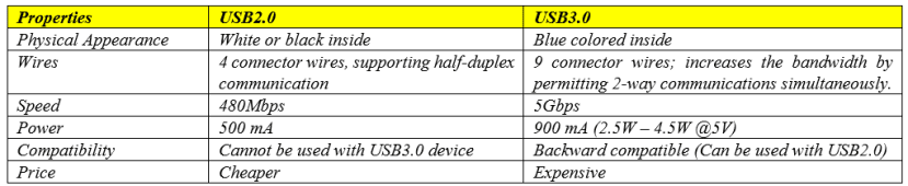
Figure 3.1: Differences of USB2.0 vs USB3.0
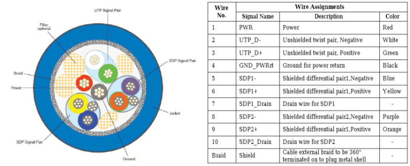
Figure 3.2: Cable cross-section vs Wire assignments illustration
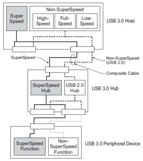
Figure 3.3: USB 3.0 BUS ARCHITECTURE
USB2.0 is a part of an existing INDUSTRIAL product portfolio. USB3.0 is developed in closing the portfolio gap. The customer base for such products is all around the globe (AP; EMEA; NA). Lead customer base is currently in AP region - Japan. USB 3.0 market worldwide have a potential of US$1 Billion.

Figure 3.4: Exploded view of USB 2.0 & Wire Schematic
2. Challenges
Customer requested deadline for first prototypes was <4 weeks. Initial concept of USB3.0 as follows.
- Process: ... ready moulding part à assembly U3 contactà assembly spacer …
- Focused on the inner core assembly process which differs between USB3.0 and USB2.0
- Remark: U3 contact can be reused. Need to develop new moulding and spacer tooling.
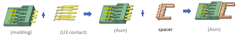

Figure 4.1: First Concept
Patent search:
- We know that there is so many patents protection on USB3.0 product. We need to investigate if the above concept is covered in some patent.
- Investigation result is that the above concept is surrounded in patent no. CN101425650BB (See Figure 4.2).

Figure 4.2: Patent Search Results
3. Results:
New concept.
- After brainstorming and several design reviews, another type of new concept was created. Please see below photo.
- Process: ... ready molding1 à assembly U3 contactà process molding2 …

Figure 5.1: New Concept
Benefits of TE Solution.
- The new concept is stable compared to the first concept. U3 contact is moulded tightly.
- Spacer part is combined into molding2 without a separated component. The structure is simply also.
- Above structure and process can avoid the patent issue.
- Above new structure, we apply for TE own patent also.
Performance:
- During the process, key points were controlled. The impedance result is within spec.
- See below photo.
- Control stripping length 2.5mm and pressing height 5.2mm will bring good impedance result.

Figure 5.2: New Concept

Figure 5.2: New Concept
- It is industrial type USB3.0, when mated with female connector, it can be mated firmly. It can offer 40 N retention force also. Please see below photo.
- It has been past the qualification test also.
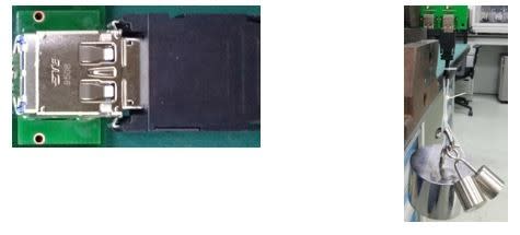
Figure 5.3: New Concept
4. Conclusion
- IND new USB3.0 plug kit can be developed successfully. It is because of good teamwork.
- Currently, the new USB3.0 plug kit product was mass production and customer placed order also.
References
[1] Bob Dunstan, “USB 3.0 Architecture Overview”, March 2010.
[2] ”TE Connectivity Patent Award Letter”, April 2020.
[3] [4] [5] Ankur Tomar, Edmud Lim, “Introduction to USB 3.0 Protocol”, vol.1, April, 2011