Hands-on with the Panasonic NFC Tag Development Kit
Follow articleHow do you feel about this article? Help us to provide better content for you.
Thank you! Your feedback has been received.
There was a problem submitting your feedback, please try again later.
What do you think of this article?
The Panasonic MN63Y12xx are a series of RFID tag ICs with built-in non-volatile memory, for use in near field communications (NFC). In this post we run through some of the examples provided with the Panasonic development kit and the SSOP packaged 1210A variant IC.
Contents
Inside the MN63Y1208 Evaluation Kit box can be found:
-
Antenna board with the MN63Y1208 NFC IC and an 8-pin connector
-
Host interface — “Micon” — control board with 8-pin connector and USB
-
USB cable
In addition to which I had the antenna board for evaluating the 1210A part, which is the one used in the examples that follow.
Setting up
Setting up the hardware is straightforward enough and simply involves connecting the antenna board to the host interface board, which is in turn connected to a Windows PC via USB.
The documentation supplied with the Windows software first takes you through installing a few external dependencies, such as the driver for the FTDI USB-serial IC used by the host interface. Note that a manual step is required after installing the 32feet.NET Bluetooth library, to copy across a DLL into the same folder as where the Panasonic NFC tool has been extracted to.
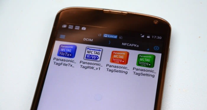
In addition to the Windows software there is also a suite of Android applications for configuring, and read/writing to and from, tags. Installing these requires you to, if only temporarily, configure your Android device to allow applications to be installed from “unknown sources”.
System
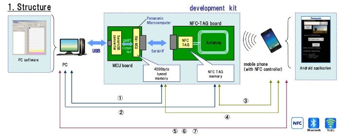
With the development system it is possible to read/write NFC TAG memory from the PC software application and an Android device with NFC. It's also possible to read from and write to the 4K “tunnel” memory which resides on the microcontroller board from either of these.
In addition files can be transferred from the Android device to the PC over NFC, Bluetooth and WiFi. In the case of the latter two NFC is used to provide pairing information.
Tag reading and writing
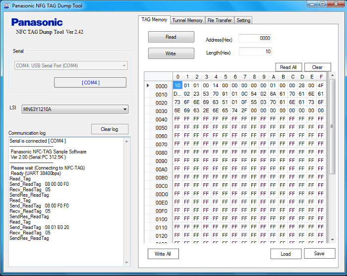
Once the PC application is started the FTDI com port is selected, followed by connect. The TAG Memory tab can then be selected, followed by read. It's then possible to modify the contents of a memory location and to write this back to the tag.
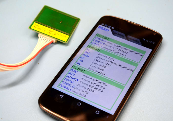
As one would expect, the tag can also be read by using the corresponding application on the Android device.
File transfer
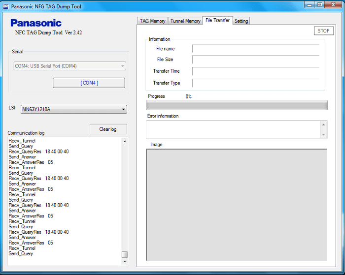
Another Android application is provided that allows you to select an image file to transfer to the PC application via one of:
-
NFC (max 900K)
-
NFC ReRAM (max 63K)
-
Bluetooth (max 10M)
-
Wi-Fi (max 10M)
The above image shows a small image file being sent from the handset via NFC ReRAM, and below this can be seen being received by the PC application.
During the course of which the address value of the “tunnel memory” currently being written is displayed on the interface board.
When transferring over Bluetooth or Wi-Fi, only the pairing information is sent over NFC.
A file transfer completed over Bluetooth
Conclusion
The antenna boards together with the host interface and companion software provide a turnkey solution for quickly evaluating the capabilities of Panasonic NFC tag ICs. With IC datasheets, application notes and evaluation board schematic diagrams available to assist those who wish to subsequently move on to prototyping solutions.




Comments