Checking heat distribution on PCB’s with the Testo 875i
Follow articleHow do you feel about this article? Help us to provide better content for you.
Thank you! Your feedback has been received.
There was a problem submitting your feedback, please try again later.
What do you think of this article?
Temperature is a key indicator when testing PCB efficiency and quality. Temperatures which are higher than expected are evidence of excessive power consumption, and if they are located in specific points could also be an indication of highly resistant contacts or internal defects in components, neither of which can be identified using electrical testing methods.
Infra-red cameras offer some significant advantages compared with more traditional contact measurement techniques. In reality, infra-red testing is the only method by which credible data can be obtained during normal operating conditions – when probes are used to test components with a low thermal mass they contribute to heat dissipation. This is because they measure the specific temperature of the heat being transferred, and not the temperature of the component itself when in operation. When PCBs are cooled by fans, obtaining accurate temperature measurements with probes is even more problematic.
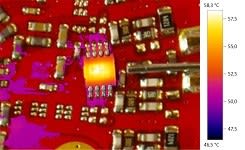
Image taken with a thermal imaging camera
Normal Image + Thermal image for highest temperatures
What features does a thermal image camera need in order to provide clear temperature measurements on a PCB?
The camera’s thermal sensitivity (NETD) and spatial resolution (IFOV) are vital.
To obtain credible data and clear images, the thermal camera needs to be capable of positioning the highest number of pixels possible on every component on the board, at least 3x3. The higher the number of pixels covering the surface under examination, the higher the number of measurements available for analysis. In reality, each pixel offers its own individual piece of measurement data, just like a virtual thermocouple which is in constant operation.
The picture below shows how to correctly measure the temperature of a capacitor on a circuit board, where 6 x7 pixels are positioned across a surface of just 0,2 x 0,3mm.
The cold parts of the component (dark) is the shiny metal reflecting ambient temperature. The part which we are interested in measuring is the silicon surface measuring 0,2 x 0,3 mm covered by 6x7 pixels (not interpolated!)
In this picture every pixel is around 30 microns – the pixel dimension is dependent on the distance at the which the image is taken from the object and the technical features of the thermal imaging camera used.
It was possible to get this result using the SuperResolution technology which makes Testo’s mid- range thermal imaging cameras highly suitable for this type of analysis, due to their capability to execute genuine algorithms.
Another important characteristic is the camera’s thermal sensitivity (NETD), especially when used on low power boards where the slightest variation in temperature can indicate a defect.
In the image below you can see how an almost indetectable heat increase can be evidence of high resistance faulty soldering. The thermal sensitivity of the thermal camera used (the Testo 875-1i) (777-6704) was just 50 mK (0,05°C/°K), which makes highly effective in the detection of minute heat differences.
The second image above clearly highlights defective soldering.
For this type of temperature measurement, the Testo 875i thermal imaging camera stands out from other solutions on the market, offering outstanding quality for a camera of its price.


Comments