DSPCBのセットアップ
ソフトウェアのダウンロード、インストール、アクティベーションの方法を学びます
初級、中級、上級と段階的にDesignSpark PCBを学べるチュートリアルです。
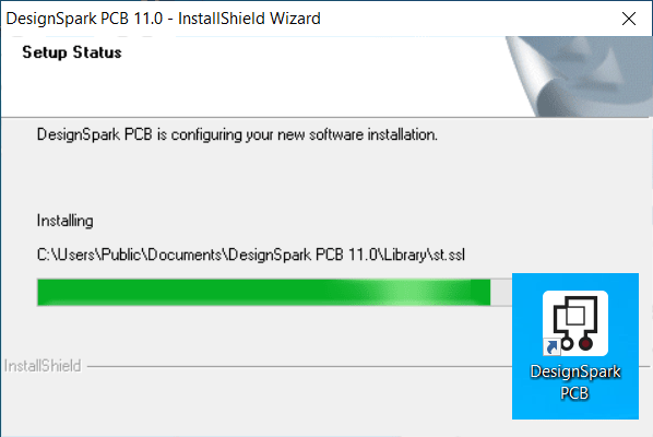
ソフトウェアのダウンロード、インストール、アクティベーションの方法を学びます
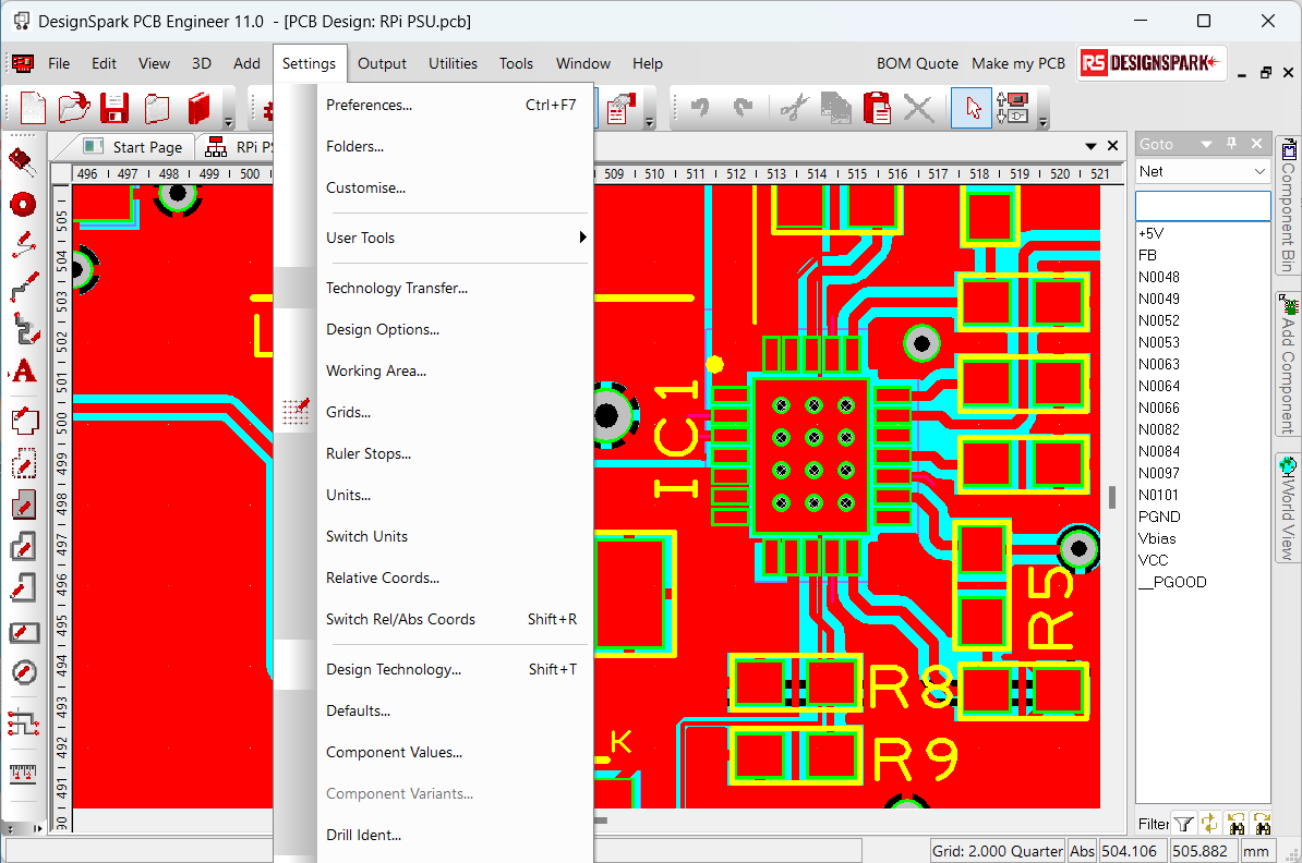
DSPCBのインターフェースや基本操作を学びます
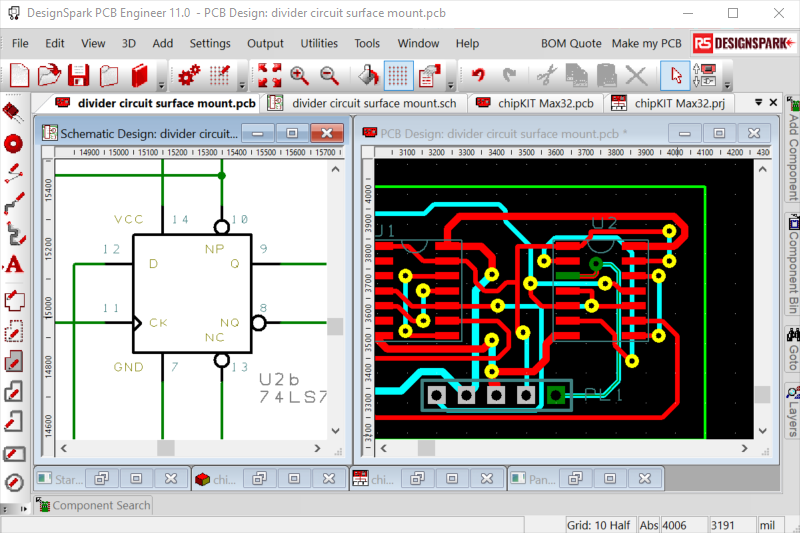
回路図から基板配線図の作成まで、新規に基板設計を初める場合の新規ファイル作成方法を学びます

コンポーネントライブラリ(基板CADライブラリ)の仕組みや作成方法について学びます
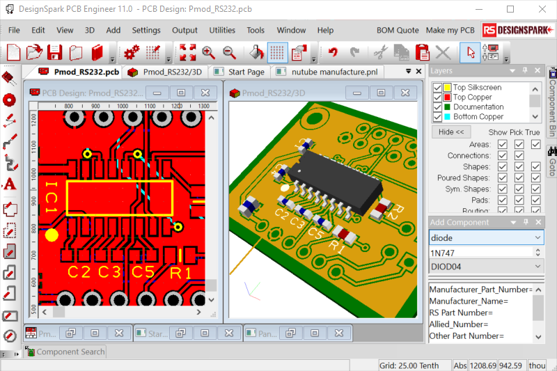
オリジナルの自作基板の設計する方法を学びます
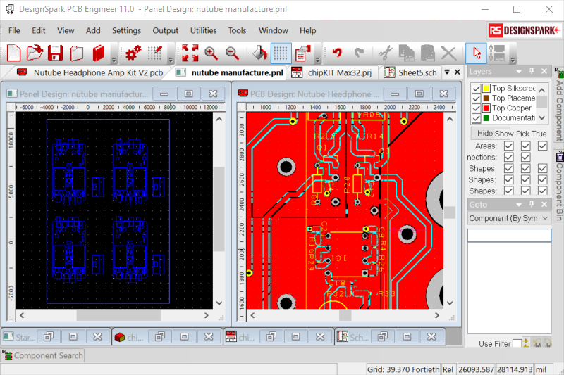
自作した基板の製造用データの出力方法を学びます。

マルチシートライセンスなら、開発チームのライセンス管理が容易になります。
DesignSpark PCBのユーザと相談できるコミュニティーです。多言語混在コミュニティーなので日本語でも投稿頂けます。