入门
了解如何下载、安装和登录软件
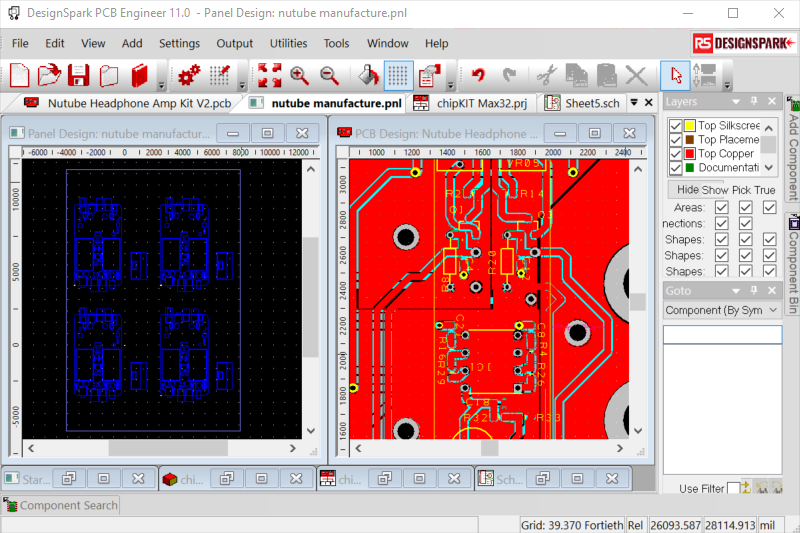
使用我们为初级、中级和高级工程师提供的分步教程,在从设计到制造的过程中先发制人
了解如何下载、安装和登录软件
学习如何浏览和使用软件内的功能
了解如何创建和构建您的第一个 PCB 设计,完成从原理图到 PCB 布局的整个过程

了解并使用 2D 模型和库
了解如何使用软件内的功能来完成您的项目设计
准备您的 PCB 设计项目,以便制造它

多席位许可证助力工程设计经理灵活把控。
寻找灵感,获得支持,并与其他 DesignSpark PCB 创作者分享您的作品。
I placed copper area on boot side and is shown in the image white color line area. I have following doubt : is the boundary line of pour area also drawn on pcb as a cooper track ? If yes then, it may short the tracks.
May anyone guide how to use cross-probes in DS PCB ? I facing a prblem that 2 XY Lines appear in place of Mouse Pointer. How to switch to default mouse cursor ? How these lines appeared ? Hello,
I have created a simple two-pin thru-hole component in a library. The reference ("RFx") works fine on the schematic (RF1, RF2, etc.), but it doesn't show up on the pcb silkscreen. How do I add the reference pcb part? Thanks Obwohl ich die anzeige der RS Startpage unter Preferences deaktiviert habe wird diese immer geladen. Das nervt. Gibt es da eine Lösung..... Hello,
We are using DesignSpark since a long time. Our IT infrastructure change and now we are behind a proxy where our IT allow access both above url :
https://tools.designspark.com/designspark/api/tools/licenseshttps://api.licensespring.com/
But we still get the error message :
They also make a rule for my computer to open queries from my computer but nothing has changed.
They ask me to contact the support of Designspark PCB to make a meeting about our issue but I can only have access to the forum.
Does someone know if the Licence server disable some range of ip address ? or someone know how to reach the support easily ? Or Does someone have an idea about our problem ?
Thanks in advance !
I am trying to cover the vias on my pcb using the solder mask however when I upload the pcb to a manufacturers website the vias are not covered. There is a post in a forum from 2019 on how to cover vias then however I cannot get it to work now. Good day
I am missing all my user created libraries. Have not recently upgraded to v 11.0. That was a long time ago.
Using the Engineer 11.0 version.
Librariy folder looks correct. On individual projects all componnets are there in the 'Current Design'. But unable to select any other libraries, including those which come with DS.
Hi,
I hope someone can help me.
I am routing a 4 layer PCB and on the top layer the tracks are showing filled as normal but on layers 2-4 the tracks are only showing as wireframe i.e no fill. I am sure the tracks are going to be filled when the gerbers are genrated but the look of it is just annoying me and I can't find where to switch these layers back to normal track view.
Can anybody point me to the area to do this?
Cheers
Kev
Hello.
I can't work out if it is possible to have different common connections on a PCB use different net styles. For instance, in my example image I have two pcb terminal blocks in paralell with high current traces and I want to "tap off" to connections that only require signal currents (for example, feeding a regulator to power a microcontroller). In my example I have had to resort to four pads to create a jumper between the two different sections of the +12v and 0V feed. If I don't seperate the connections they seem to only be allowed one net style. Is there a better way?
I usually save my PCB Plots to a folder below the Design File, normall just called 'PCB Plots' which I would set in the options dialogue window. However, having just moved from Explorer to the Creator subscription, I find that the "This folder below the design file:" box is greyed out and permanently set to a recently used folder which is not appropriate for current and future designs. I do not have the Compose button to its right either to set up the file naming parameters as the Help File suggests I should.
I have searched the registry and found the PlotSubdir entry pertaining to the unchangeable recent entry, which I could manually change as a workaround if necessary, but it shouldn't be necessary of course.
DSPCB is fully up to date including the February 23rd patch, and runs happily on my 15-year old Windows 7 x64 system. I intend to update to a new PC in the near future and obviously to Win 11.
Do I need to reinstall DSPCB and apply the patch again to recover this in the meantime?
Any guidance on a fix is most welcome.
Thanks Bonjour,
Je ne comprends pas pourquoi il y a ces liaisons en trait fin jaune. Je n'ai pas créé ces liaisons, et même si je les enlève, elles réapparaissent automatiquement.
Merci d'avance.
I have a mystery on my hands. The highlight trace is the step pulse for the stepper motor driver ( DRV8826 ). When I attach the O-Scope probe to the stepper test point ( The via on the trace ) it runs wild!!!! Then when I move my hand it also causes the stepper motor to run eraclicy. Denping where my hand is it runs slowly or very violent steps!! Even with the probe disconnected.
Does anyone have a clue what's causing the weird behavior?
If you're wondering about the large hole, there for fan mounts.
The step pulse is generated by the logic controller (Adafruit Itsy Bitsy 32U4 3V GPIO Pin 5 ). how to switch language?such as Chinese Bonjour,
J'ai réalisé une PCB de 5 couches.
Pourquoi les couches ' Gnd Plane et Vcc Plane ' ne contient pas des pistes ?
Est ce que je peux supprimé les deux couches Gnd Plane et Vcc Plane ?
Merci d'avance
copper pour boundary
Cross Probe use in DS PCB
Crossed XY Lines in PCB Layout
Component Ref not showing on PCB silkscreen
Startpage
Can't reach licence server with proxy
How to cover vias
Missing user created libraries
Tracks Wireframe Only
Mix different net styles to common connections
PCB Plot files location problem - Creator edition. Cannot set Sub Directory for plots
Fausse liaison
Noisy Trace Mystery
how to switch language?such as Chinese
Gnd Plane et Vcc Plane