Explanation of Component Spacing DRC Reports
Follow tutorial
 Dave from DesignSpark
How do you feel about this tutorial? Help us to provide better content for you.
Dave from DesignSpark
Thank you! Your feedback has been received.
Dave from DesignSpark
There was a problem submitting your feedback, please try again later.
Dave from DesignSpark
What do you think of this tutorial?
This tutorial requires:
DesignSpark PCB V11.0.0The following is an in-depth discussion from the DesignSpark article: Mind the gap! Component spacing in DSPCB
It can be confusing at first as to what is reported by the Design Rules Check as a component spacing issue requiring you to examine.
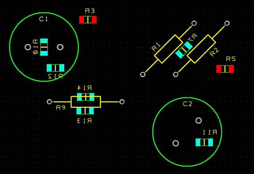
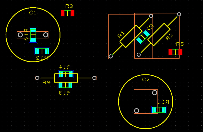
Below is a simple example showing some components and placements where this will occur.
In this image, the through-hole components are on the top layer and all surface mount components except R3 and R5 are on the bottom layer. From this visually you will not expect any component spacing issues.
Running the DRC you may be surprised to get issues reported as shown below.
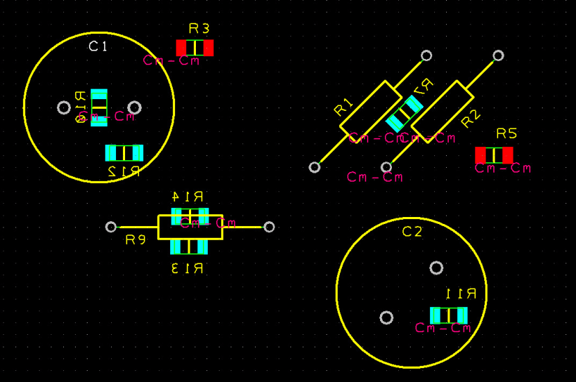
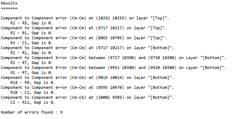
The report showing these as a zero gap when clearly it is not.
The reason this occurs is DesignSpark PCB and Pro use a simplified model when performing the "Component Spacing" checks in the Design Rules Check.
What is this simplified model?
The majority of PCB designs are using components placed on the board in an X,Y orientation, the simplified assumption is the component is considered to be contained in an area that encloses all the pins and silkscreen markings. This rectangular area is referred to as the "Bounding Box" and works very well for the majority of rectangular components, however you need to be aware of where it can give false warnings from the DRC as illustrated above.
The image below illustrates the bounding box in purple used for the spacing check for the Top layer.
This illustrates two issues, firstly non-rectangular components such as C1 have an enlarged footprint when bounded by a rectangle. Secondly, a component placed at an angle can have a much larger footprint. In these instances, R3 and R5 are reported as "Gap is zero" as they encroach into the space assumed for the other component.
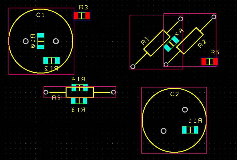
The image below illustrates the bounding box in orange used for the spacing check for the Bottom layer.
As through-hole components do not have any of the physical components on the bottom layer a bounding box enclosing all the pads is used.
This again illustrates some issues; the area that is considered to be the "spacing" footprint will be long and thin, so will report issues for R14, but not r13 below R9.
The resistors R1 and R2 and the capacitor C2 have a much larger footprint than may be expected causing unexpected DRC issues as shown in the previous report.
Can this model be improved to reduce these false positive reports?
The answer is "Yes" and detailed in another article listed below regarding "Placement Layers and Shapes", however now you understand the limitations you need to decide will your layout be affected and is a visual check plus the use of the measuring tool a suitable alternative.
If your design has all the components mounted on the top copper side and you are using rectangular components placed orthogonally you are unlikely to have any false spacing reports. The exception being cylindrical components with radial connections.
If you are placing surface mount components on the bottom copper side then any spacing issues reported with components on the top copper side can generally be ignored as track and pad spacing checks in the DRC will report most issues of concern.
Are there any concerns if you just use surface mount components?
Generally no as most footprints are rectangular and the bounding box is on the component side only and there are no interactions between top and bottom layer components.
The exception is if you mount components at an angle and for these you may benefit from a placement shape on the placement layer.
Summary.
The bounding box issues affect four main areas.
1. If the component is mounted at an angle. This is becoming a more common issue as PCBs are often no longer rectangular in shape and may be circular, semi-circular or any free shape. As an example a digital 'analogue' clock face or dial may have resistors and LEDs placed radial from the center of the board.
The bounding shape around for example a resistor placed at 45 degrees will be much larger than in the X,Y placement.
2. If the component is not of a rectangular shape. The classic examples are cylindrical components such as radial capacitors.
3. The component is a module placed above your main PCB. Examples are an LCD display, microcontroller modules such as mBed and Arduino Nano or any 'daughter board' used for sensors, networks, IoT etc. However, as the PCB design will often use SIL connectors these may not be an issue.
4. Your PCB is double-sided and contains surface mount components underneath through-hole components. The reason this generates DRC component spacing issues is that a through-hole component by default has the bounding box on solder side enclosing the pads. However, this may be desirable to prevent components being placed between higher voltage pads on a component.
Additional reading
How to create a placement layer and add a placement shape to a component?