Mind the gap! Component spacing in DSPCB
Follow article
 Dave from DesignSpark
How do you feel about this article? Help us to provide better content for you.
Dave from DesignSpark
Thank you! Your feedback has been received.
Dave from DesignSpark
There was a problem submitting your feedback, please try again later.
Dave from DesignSpark
What do you think of this article?
The component to component spacing Design Rules Check by default calculates the size of a component by calculating a "bounding" box that contains the component footprint and silkscreen markings.
This performs well for many components as shown in this example PCB.
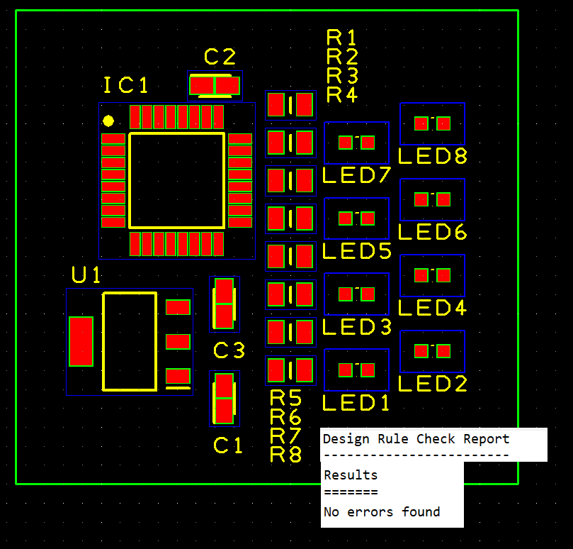
The bounding box calculated for the components as placed on the PCB plus the required "spacings" set in the Design Technology results in no errors being detected.
So where does this simplified model fail?
The following example PCB with the same spacing values in the rules illustrates where to aware of potential issues.

Here we have 34 error reports of "Gap is 0".
Visually there is very good spacing, so where is the issue?
The issues result from the bounding box being calculated around the component on the PCB in the X,Y plane. This impacts on many of the components shown and the usual surprise is with cylindrical components such as LS1,2 and C1 where the bounding box is actually a rectangle. It also occurs with components placed at an angle, such as IC2 and the others.
The second issue is the bottom layer bounding box for a through hole component is one that will contain all of the pads. In the image, LS2 has a much larger size than LS1 and the resistors R1..R3 result in very large bounding boxes.
Full details of this and tips are detailed in this article.
What if you need an enhanced check to perform a true spacing check?
This can be resolved by adding your own shape to components as a "Placement Shape".
The outline of the component is added to the Top and Bottom "Placement Layer" of the library component for a through hole part or just the top for a surface mount part.
For through hole components the bottom placement shapes can be placed around the pads to allow SMD's to be positioned between pads if required.
Once the PCB Design Technology is set to include Placement Layers and the parts have a Placement Shape this overrides the default bounding box calculation for those parts and removes these error reports.
Full details can be found here.
As discussed only certain components and orientations will require you to use placement shapes.
Important additional information.
For users of PCB Part Library, many parts from SamacSys will have a placement shape which will be loaded onto the "Documentation" layers. Setting the Documentation "Layer Type" to be of type "Placement" will allow SMD's to be placed at angles with correct spacings calculated. This can save you considerable time.