How to create a placement layer and add a placement shape to a component?
关注教程
 戴夫来自 DesignSpark
How do you feel about this tutorial? Help us to provide better content for you.
戴夫来自 DesignSpark
Thank you! Your feedback has been received.
戴夫来自 DesignSpark
There was a problem submitting your feedback, please try again later.
戴夫来自 DesignSpark
What do you think of this tutorial?
本教程需要:
DesignSpark PCB V11.0.0The following is an in-depth discussion from the DesignSpark article: Mind the gap! Component spacing in DSPCB
Placement Shapes.
Having considered the points in the previous tutorial [please read this first] you decide that you require an improvement to the component spacing check in the DRC. This is achieved in DSPCB by modifying the library component footprint to include a "Placement" shape that represents the actual component area.
For advanced users these are the required steps:
1. Create a new "Layer Type" Placement.
2. Create new Layers for top and bottom Placement shapes.
3. Add placement shapes to your components.
Note. You may also benefit from the details below which describe the component shape on the documentation layer of components downloaded using our PCB Part Library
For those who would prefer step by step instructions please follow the suggestions below:
In DSPCB, you then need to add a "Placement layers" to your Design Technology of <type> "Placement" and these will be used where the component has the feature added.
The followings takes you through the required steps with examples.
Adding a Placement Layer to your design.
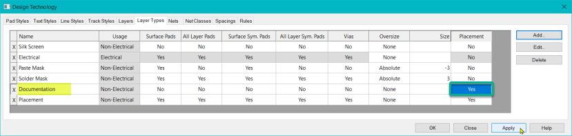
Launch the Design Technology window by shortcut SHIFT+T and select the <Layer Types> tab as shown below.
You may have other Layer type names depending on your previous settings, but if you do not have a "Placement" type, click <Add> and complete the form that opens as shown and click <OK> to add to the types.
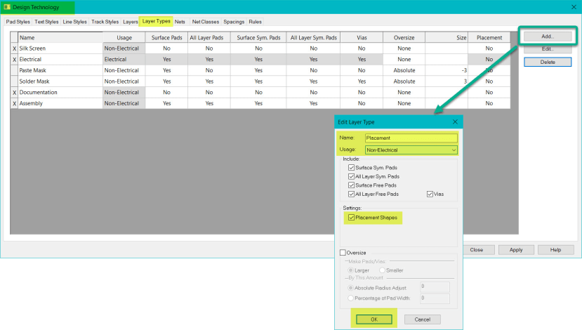
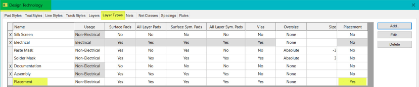
Your types list will now appear as below.
Note that in the <Placement> column the entry for the new Placement Layer Type is set to "Yes".
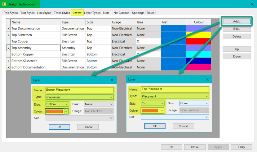
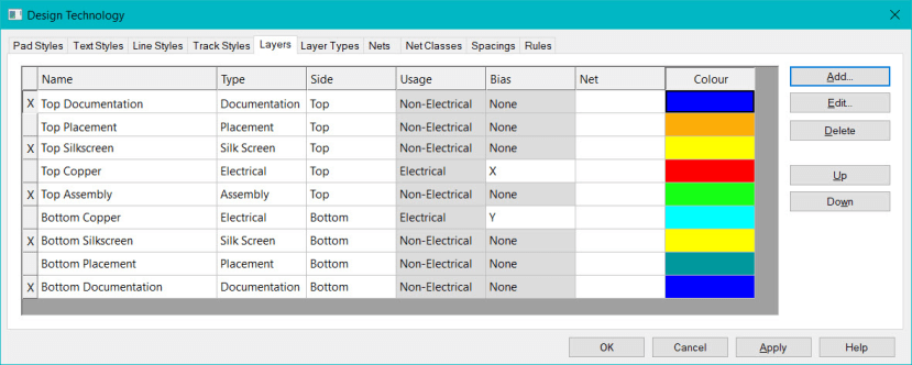
Now select the <Layers> tab and we will add new layers of type "Placement".
This has to be done twice to add both a Top and Bottom placement layer.
You can add a colour at this point or later to distinguish from your other layer colours.
After these are added your list will appear as below showing your new layer entries.
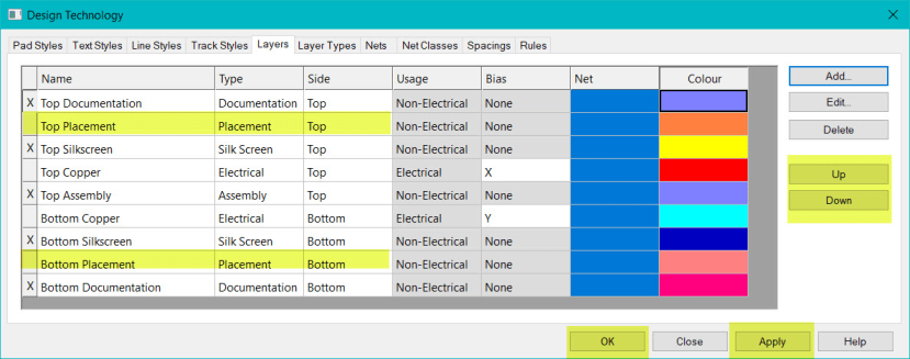
You can select a layer and use the <Up> and <Down> buttons to order as required and also change the colours for a clearer PCB view as shown in the example below.
Now click <Apply> and then <OK> to close.
Your Design Technology settings are now ready to use with component placement shapes which need to be added to the required component footprint in the library.
To save having to perform the above for each new design save these settings as a new Technology file.
From the menu bar select File - Save Technology File and then complete the "Save as" form.

Give the technology file a new descriptive name so as not to overwrite the existing ones.
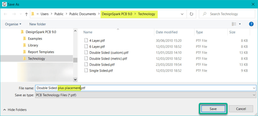
You will now be able to use this technology file the next time that you start as new PCB design.
Now to customise the component footprints to include placement shapes.
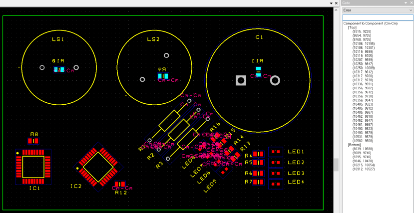
The following PCB layout uses components downloaded from PCB Part Library as examples to illustrate typically where a placement shape will be of benefit. Visually examining this layout there are no obvious placement errors.
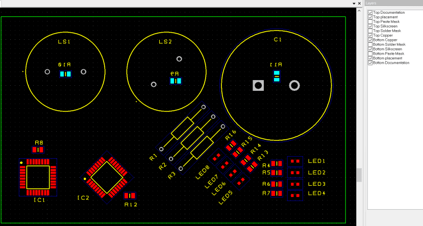
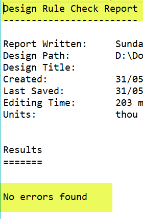
Running the Design Rules Check for "Component Spacing however reports 34 Issues!
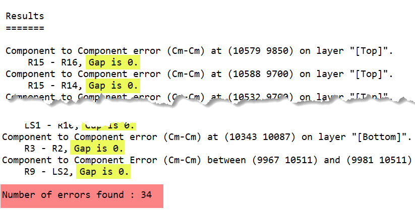
All are reported as "Gap is 0" and clearly this is not the case.
Now edit the components to include a placement shape.
Starting with LS1 and 2 select the component and right-click, from the context menu select Edit Component in the Library.
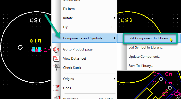
The Library Manager now opens for this component.
Place the mouse pointer over the PCB footprint, right click and select <Edit PCB Symbol>
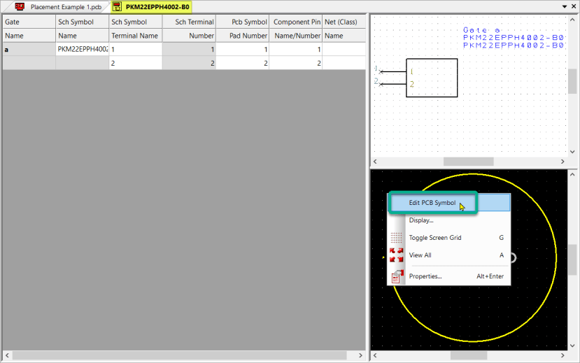
In the footprint editor you can now add Placement shapes to the footprint.
See Note 1 at the end of this article if you cannot perform this task.
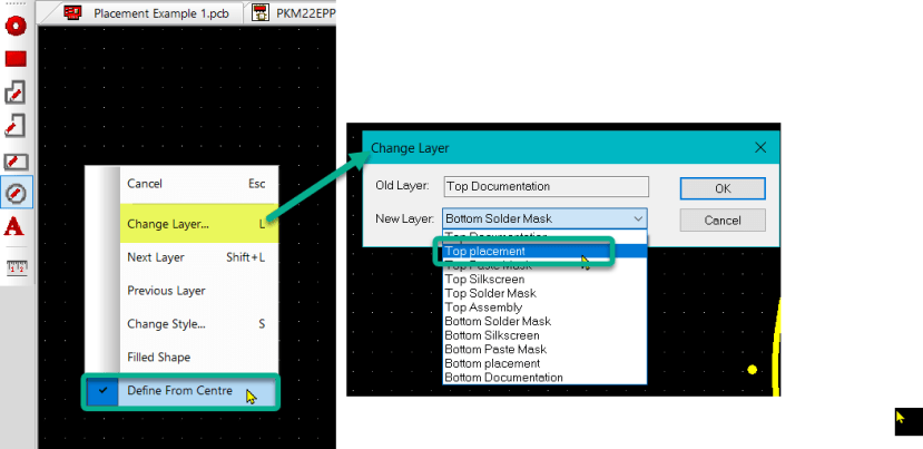
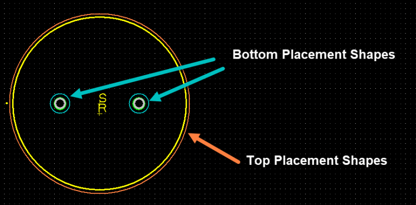
We now add circles to the Placement Layers, for the top side this is the whole component and for the bottom side we use the pads. Select the circle shape from the Toolbar, right-click and check the <Define from Centre> is ticked, then select <Change Layer> and select "Top Placement" or "Bottom Placement" as required and add the shapes.
Here is our example footprint with placement shapes on the appropriate layer.
Click [Save] from the icon to save the new symbol.
This will ask for the footprint/symbol name. As we are adding to the current footprint just select OK and "Yes" to overwrite with the updated footprint.

Close this tab and now from the Component editor tab, again click the "Save" icon and "Yes" to overwrite and update the component.
The component in the library is now updated and can be used as before in your designs with or without a placement layer.
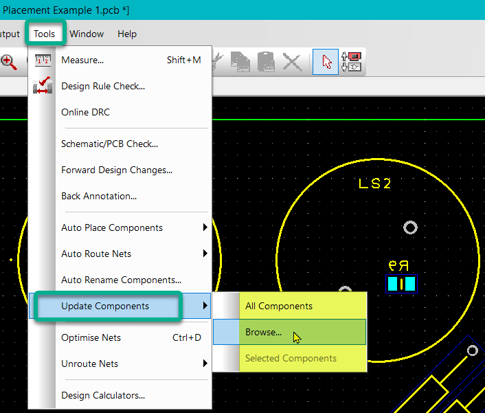
To use this new component you can either update all components or update individual or selected components.
After the update and performing a DRC some of the error warnings are now removed.
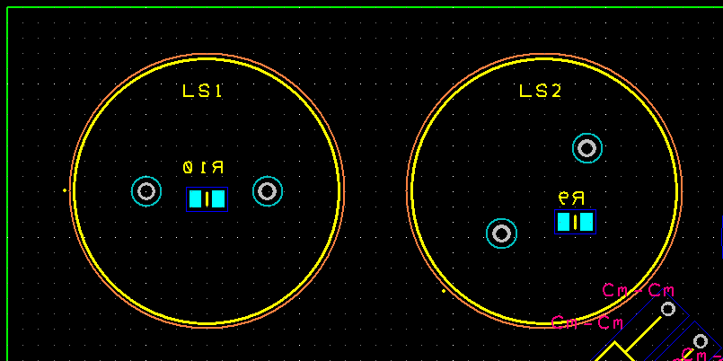
Repeat these steps for the other through-hole components.
Here we update the the axial resistors and illustrate that the placement shape can be a complex shape. This is only to illustrate that shape can be adapted to match your requirements and would not normally be required for a resistor.

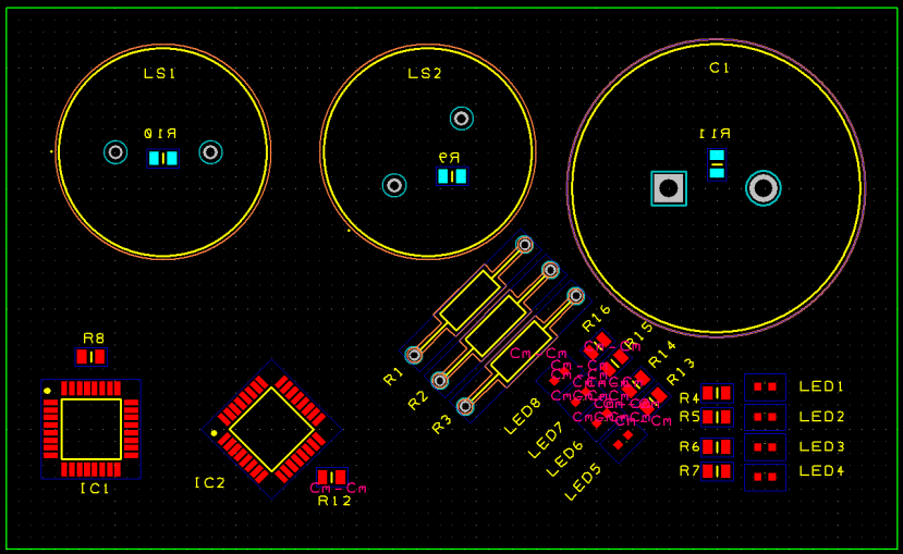
Updating the components from the library all the through-hole components now have a top and bottom placement shape and a DRC shows the number of errors is significantly reduced.
What remains are the Surface Mount components positioned at an angle which have a large bounding box as previously described here.
Components downloaded using PPL have a shape on the Top/Bottom Documentation layer which can be used as a Placement Shape. Launching the Design Technology and selecting the <Layer Types> tab we can assign this as another Placement Layer as shown below..
When the DRC is now performed no errors are reported.
It is up to you to decide whether these supplied shapes meet your requirements, but if they do this will save you the time required to create your own dedicated placement shapes.
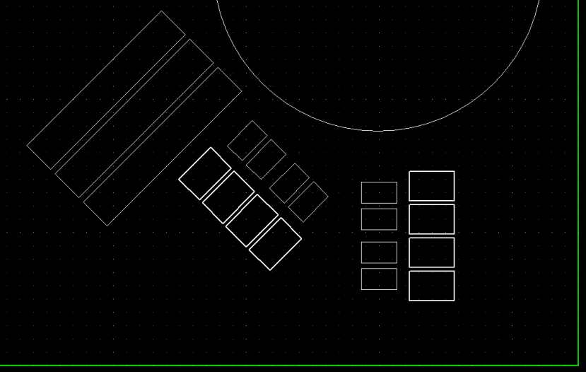
This image shows the Placement Shapes (in white for clarity) on the documentation layers supplied from PPL. These could also be used for through-hole components which would then only require the pads on the bottom copper being defined.
Summary
With your own placement shapes, or in combination with those from the PPL supplied components you can enhance the accuracy of the Component to Component spacing check in the DRC.
Adding your own placement shape is quick and can be customised to your own design requirements.
Note 1:
It is possible that you do not see a placement layer when editing the footprint symbol.
This can be enabled by launching the Library Manager and selecting the [PCB Symbols] tab and then the "Tech Files" button. Select the required Technology File with a Placement Shape layer and this will be used in the component preview pane and importantly in the footprint symbol when being edited.
