Frequency Analysis for Embedded Microcontrollers, Part 6
Follow article
 Dave from DesignSpark
How do you feel about this article? Help us to provide better content for you.
Dave from DesignSpark
Thank you! Your feedback has been received.
Dave from DesignSpark
There was a problem submitting your feedback, please try again later.
Dave from DesignSpark
What do you think of this article?

My test rig for the dsPIC-based embedded spectrum analyser project. The DSO on the left is displaying the output from the function generator: a classic Sin(x)/x or Sinc(x) waveform. Its frequency spectrum produced by the FFT running on the Clicker 2, appears on the laptop screen on the right. The MikroElektronika Clicker 2 (144-8343) is in the centre next to the MikroProg program/debug unit (791-6347) .
While waiting for a suitable LCD display board to come back into stock, I’ve been playing about with the sampling rate and dB display formats on my dsPIC-based spectrum analyser.
Linear v Decibel display format
An irritating feature of simple linear spectral power displays is the tendency for one large component, usually the zero-frequency or dc-offset, to dominate the automatic scaling software causing all other frequencies to be reduced to near invisibility. There are three ways of dealing with this problem:
- Clear the zero-frequency power component after the FFT calculation, but before the output scaling takes place. This is effective in most cases because the dc offset is of no interest relative to the ac components, but it’s frequently the largest! Analogue to Digital Converters (ADC) generally cannot handle bipolar signals, so a circuit must be added to the analogue input ensuring it’s always positive – hence the exaggerated dc offset value.
- Calculate and display the square-root of the FFT output samples yielding results proportional to voltage V rather than power V2.
- Convert the linear output to a logarithmic base 10 format, with units of decibels or dB.
Solution No. 1 is useful but limited to spectra dominated by the 0 Hz component only. It might be worth including as a panel-switch option. I used approach No. 2 for the printouts in Part 5 of this series. It’s good for situations where you need to have an output in terms of voltage relationships. To see the effect of solution no. 3, take a look at Fig.1.

In Fig.1a we have the linear power spectrum of my favourite test waveform: a 50:50 mark/space ratio pulse train, aka a ‘square’ wave. It’s ideal because the output spectrum only consists of a ‘fundamental’ frequency – the same as the pulse repetition rate – and a series of ‘odd’ harmonics decreasing in amplitude. Not forgetting the dc offset, of course. Usefully, the voltage amplitude (square-root) of each harmonic should be the fundamental’s amplitude divided by the harmonic’s order. So, the 3rd harmonic is one-third the size of the fundamental, 5th harmonic one fifth, 7th harmonic one seventh and so on. In the graph shown, notice how scaling the huge dc offset has ‘flattened’ the displayed harmonics.
Now look at Fig.1b, where the shape of the spectral envelope is much clearer thanks to the logarithmic vertical axis. The negative numbers (with the units of dBs) indicate the power level relative to the largest component, in this case the dc offset, which is assigned the value 0 dB.
Calculating decibels
The subject of decibels tends to be surrounded by a fog of confusion and misunderstanding, leading to mistakes when attempting actual calculations. I attempted to tackle this confusion last year in a DesignSpark article entitled: The Decibel – What’s it for? , so I won’t go through all the details again here except to reproduce the basic equations:
GdB = 10log10(P1/P2) dB where P1 and P2 are signal powers in Watts. GdB is a power ratio in dB.
Now P = V2/R watts where V is signal voltage in Volts and R is the resistance in Ohms.
So GdB = 10log10(V12/V22) dB where V1 and V2 are signal magnitudes in Volts. The R values cancel out because they are normally designed to have the same value. This leads to:
GdB = 20log10(V1/V2) dB by taking the ‘square’ term outside of the log10 function where it becomes a multiply by 2 instead. Note that the result G is still the same power ratio in dB. The formula using 20log10 is frequently used for the practical reason that it’s easier to measure voltage in a circuit than power.
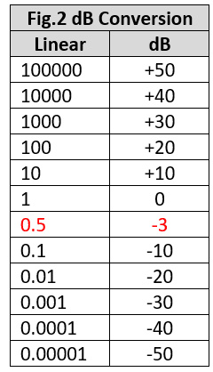
G is used as the variable name because the ‘Gain’ or amplification of a circuit is often expressed in dBs where P2 = PIN and P1 = POUT. Notice that G is negative if P1 < P2, in other words, a ‘Loss’ rather than a Gain. I’ve included a basic linear-power to dB conversion table (Fig.2) to show how very large or very small ratios are compressed into something more manageable. The value for 0.5 is particularly important as it comes up again and again when discussing the frequency response of circuits such as amplifiers and filters. Yes, it’s the ‘3 dB point’ on a plot of amplifier Gain (or filter Loss) indicating the frequency at which the power output has reduced by half.
Logarithms without Floating Point arithmetic
The numbers emerging from the FFT are of unsigned 16-bit format, representing Power P. To calculate relative power in dBs we are going to need a reference value representing 0 dB. This will be 65535 in this case because it’s the largest unsigned 16-bit number. So, our dB formula becomes:
GdB = 10log10(P/65535) dB
When P = 65535, we get GdB = 0. Smaller values of P yield negative results indicating their value in dB relative to 0. Now for the hard bit: how do you calculate the log with only integer arithmetic and no ‘scientific’ functions available in the MCU instruction set? Fortunately, I came across this academic paper, Quick and Easy Binary to dB Conversion, which even had a code listing for a software routine in 8051 MCU assembly language. It didn’t take long to convert it to dsPIC33 code. The only modification to the algorithm was to divide the result by 2 to take into account my use of power measurements rather than voltage as used in the article. The dsPIC version of the source code is available in the Download section below.
The algorithm assumes the reference level to be the largest 16-bit number (65535), but it’s rather more useful to assign the 0 dB value to the largest number in the actual data. To that end, the code following the dB converter processes the data, making the largest 0 dB while displaying the rest in order of increasing negativity. As a result, the minimum value is never going to be less than -48 dB – equivalent to a power level of 1.
Faster, but less accurate
You may have noticed in these examples that the sampling frequency has been increased to 1 MHz (1.048576 MHz to be precise). I thought I would push the dsPIC’s ADC to its limit, albeit with a reduction in amplitude resolution from 12 to 10 bits. With a window length of only 256, that leaves a measured frequency resolution of 4096 Hz. The window will have to go up to at least 1024 to reduce that, and my analyser will need a switchable sampling rate facility to get meaningful results down at audio frequencies.
Acting on Impulse
I’ve said that my favourite test waveform for this project is the 50% mark-space ratio rectangular pulse train. But what happens when the pulse period is steadily decreased down to a single sample period? This is what I’ve done in Fig.3: starting with 50% and halving it each time down to 3.125%. The final step, 0.39% takes the pulse width down to a single sample period. The 50% case is ‘special’ because its symmetry ensures there are no ‘invisible’ frequencies. Notice how, as the pulse width halves, the lobe widths double until by [f], the primary lobe is so wide it appears flat as far as the Nyquist limit at bin number 128.
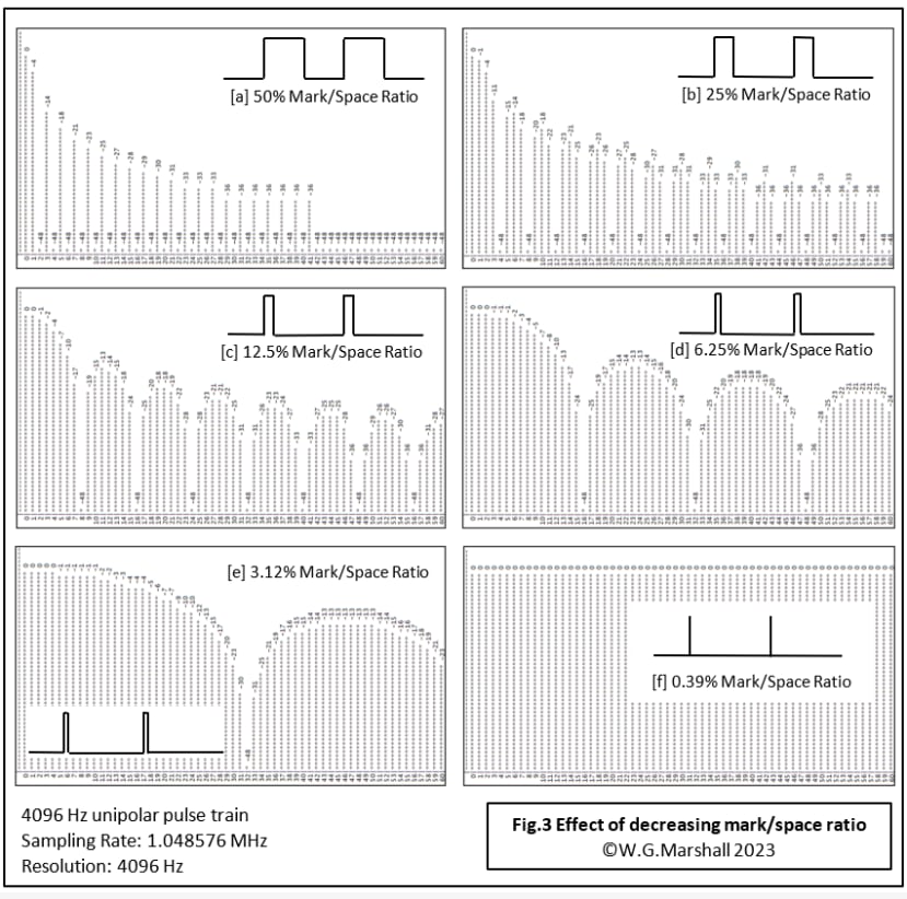
What we have here in [f] is a practical realisation of the Impulse Function, which in theory contains all possible frequencies. But only when it has zero width. If such a pulse is applied to a mechanical, or electronic circuit such as an analogue filter, the output is unsurprisingly, referred to as an Impulse Response. Because the input pulse contains all possible frequencies, the output pulse contains all the information necessary to characterise the circuit’s frequency response. The latter can be determined by running the sampled impulse response through an FFT. As it happens, the input pulse need not be zero width, as long as it’s a lot narrower than the impulse response output. This is what is happening in the heading picture: the function generator is producing a synthesised impulse response in the form of a Sinc(x) function with a repetition frequency of 8.192 kHz. The signal is processed by the FFT program on the laptop to reveal the frequency content. Looks like a low-pass filter, flat until it rolls off at 81.92 kHz, doesn’t it? In a future article, I’ll cover how to derive the impulse response from a desired frequency response, creating the tap-gains necessary to make a Finite Impulse Response (FIR) digital filter.
If you're stuck for something to do, follow my posts on Twitter (X). I link to interesting articles on new electronics and related technologies, retweeting posts I spot about robots, space exploration and other issues. To see my back catalogue of recent DesignSpark blog posts type “billsblog” into the Search box above.