The link between ESD and EMI
Follow article
 Dave from DesignSpark
How do you feel about this article? Help us to provide better content for you.
Dave from DesignSpark
Thank you! Your feedback has been received.
Dave from DesignSpark
There was a problem submitting your feedback, please try again later.
Dave from DesignSpark
What do you think of this article?
Introduction to ESD and EMI
Current Electrostatic Discharge (ESD) control practices have substantially minimised the dangers from unwanted electrical overstresses that are known to haunt semiconductors and other micro-electrical devices at all stages of their manufacturing, handling and applications.
The act of grounding an ungrounded ESD Sensitive (ESDS) device can trigger an ESD event, yielding latent or catastrophic damage by means of an energy or voltage failure mechanism in the ESDS device. To minimise this potential problem, the rate of discharge must be controlled during grounding and the work potential at the grounding electrode must be increased [1]. Decreasing the rate of discharge will limit the current density of a potential electrical arc (ESD event). Any combination of an increase in resistance or capacitance in the contacting electrodes (the two materials that sustain a discharge) can decrease the rate of discharge and lessen the effects of an ESD Event.
One of the side effects from an electrostatic discharge (ESD) is an induced EMI (Electromagnetic Interference). An ESD-induced EMI in the near-vicinity of mission-critical equipment can cause data errors, temporary resets or even power-up resets requiring operator intervention [2]. This is caused by the EMI undergoing conversion to a voltage or current, which in turn corrupts the operation of the circuit/logic inputs.
The effects from undesired electromagnetic radiation, EMI, on ungrounded or unshielded conductors is commonly underestimated. An ESD event occurring outside an ESDS protective work area can still pose a risk to unshielded and ungrounded conductors within the critical work or ESDS area.
Case Examples of ESD/EMI Problems
Some examples of ESD/EMI problems reported from the Center for Devices and Radiological Health (CDRH) databases are listed by product recall numbers. Recall numbers M485337, M485338, M562311 (March 1994) state that static from bed sheets when a nurse was making the bed caused infusion pumps to sound a "processor lock-up alarm". Recall number M249358 (October 1991) states that a discharge from an operator to the timer of a radiation therapy system caused the timer’s display to blank just as treatment began. Recall numbers Z3112, Z3212, Z3132, Z142 (January 1992) state that ESD affected infant radiant warmers, causing the heater to turn on or off, the alarm not to activate, and the display to become blank or corrupted, [9].
Today's TTL and CMOS logic states have a logic "0" at 0.8 Volts or lower and a logic "1" at 2.0 Volts or higher. This leads to a smaller indeterminate range of 1.2 Volts for most TTL and some CMOS logic circuits and places the logic inputs from these circuit traces or cable connections susceptible to induced EMI voltages exceeding this range. One example of an ESD-induced EMI was characterised from office chairs [3, 4]. Induced voltages over 2 Volts have been measured on a printed circuit assembly (PCA) 90 cm from the furniture ESD [4]. 2 Volts is enough voltage to easily drive a TTL circuit let alone an ECL circuit into a logic error.
Table I lists some logic devices and their potential susceptibility to EM energies. Noise margin is a quantitative measure of a device’s noise immunity. The high-level DC noise margin in Table I is the difference between the minimum device output levels for a logic high VOH of the driving gate and the minimum input level VIH required by the driven gate to recognise a "1" logic state. The Indeterminate Range is the difference between the logic inputs’ low level maximum and high level minimum to differentiate between a logic "0" or "1".
Some types of common lab stools and office chairs can radiate a series of impulsive fields from metal legs due to internal ESD when a person rises from the chair. As many as 12 pulses have been recorded within a 10 second period after a person rises from a chair [3]. Smith stated that a value of tens of millivolts per inch (~2 V/m) is generally not enough to affect digital logic whereas values over one volt/inch (40 V/m) are potential problems. One example observed induced voltages of over 4 volts/inch (>160 V/m) in cables one foot from one type of office chair [3].

Table I - Table of Logic Families’ Power Transition, Noise Margin, and Indeterminate Range [8]
What often looks like software errors in process equipment may actually be caused by an external static charge (or discharge) problem. An ESD event anywhere in a room can cause an EMI. That EMI can couple into a system through cables or open chassis and induce a noise voltage greater than the logic inputs’ indeterminate range and cause a single event upset. EMI effects to microprocessors or other circuit logic latch-ups in process equipment can manifest itself in several ways, such as random hangs, robotic malfunction, or software errors, all resulting in downtime and reduced throughput.
Theoretical Energy Analysis
1. Mechanism of an ESD Event
There are three well-known methods to simulate an ESD Event: the human body model, the machine model and the charge device model. Each has its place to aid in designing the proper ESD Control Programme depending on the application.
Induced voltage from an EMI energy transfer to a logic input trace with typical area of 40mm2 could be as high as 485mV with an ESD-induced 100 MV/m field at 33cm as depicted in Table II. 485mV is enough voltage to flip a logic state of an ECL device as depicted in Table I. From the same ESD event, a data input cable with a receiving area of 40 cm2 can have an EMI-induced voltage of 4.85 which is enough voltage to drive a logic error in any family or subfamily of logic circuits; TTL, CMOS, & ECL.
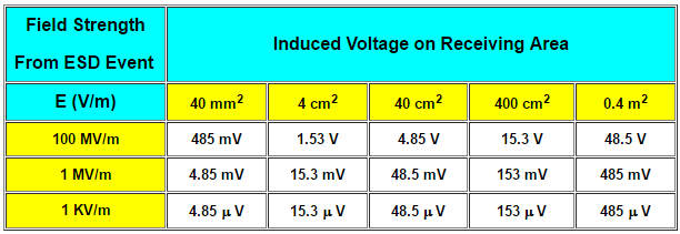
Table II - EMI Energy Transfer from an ESD to an Isolated Conductor using antenna theory where: the area of the conductor is A=variable, the distance from the source is R=1/3 meter, ESD has a 1 ns rise time and a 3 ns pulse width.
2. ESD Event
An ESD event can have a fast rise time, especially for low voltage discharges [5]. The waveform for an ESD event includes high-frequency components with a frequency range from DC to over 6GHz, [4]. This electromagnetic radiation (EM) can readily couple to circuit traces (conductors acting as antennae). For ungrounded conductors coupled within a capacitive circuit, this EM wave can induce a static charge, building until a discharge, breakdown, recombination or neutralisation occurs. High-speed circuits, by their nature, tend to be very susceptible to high-frequency signals such as those from a nearby ESD event.
The electrostatic field strength (Eo) just before an ESD is proportional to the charged voltage (V) at gap width δ. The gap width, δ, is defined by Paschen’s Law, but may vary in each discharge condition. The electric field strength Eo = V/δ where V is from 0.5kV to 30kV and δ is from 5μm to10mm, can yield an electric field strength as high as 6 GV/m. This extremely high field strength is attributed to a smaller gap width, δ = 5μm. It is important to note that the arc length of an ESD is of greater influence to its disturbance than its voltage [7].
3. EMI
An Electromagnetic Interference (EMI) is an unwanted electromagnetic energy, (whether intentionally or unintentionally generated), of almost any frequency and energy level. EMI is defined to exist when undesirable voltages or currents are present to adversely influence the performance of an electronic circuit or system. Sources of radiated electromagnetic energy from ESD are very common in today’s factories from furniture ESD, raised flooring ESD, Human Body ESD, hand held toolbox ESD and metal-to-metal ESD [3, 4, 6, 7]. An EMI, or summation of EMIs, can over time induce a charge (static voltage) on an ungrounded conductor coupled in a capacitive circuit, i.e., an isolated capacitor. An even more common occurrence is a single ESD induced EMI that can upset a logic circuit and cause systems errors. The very fast rise time of an ESD may be preserved if it flows through a metal conductor, resulting in radiated EMI.
Solutions
- Assume that all electronic devices are susceptible to damage or logic error states from ESD and EMI, respectively; and take the proper precautions.
- Proper grounding of isolated conductors and use of ground-planes near active conductors will minimise some of these effects.
- Shielding the known emitting devices will help, but it is the unknown emitters that will cause the most problems. Thus, shielding the receptors, sensitive logic devices, will help combat EMI-induced logic errors. Start shielding at the device level, for it is less costly than at the system level.
- Reduce ground-loop areas between interconnected equipment and systems. Route interconnected cables inside conduit, cable trays or raceways when possible. Do not coil excess cable into a helix, but rather fold back and forth to foil antenna gains.
- Metal-to-metal discharges will always derive the largest current derivatives (di/dt) and hence generate the strongest EMI fields. Treat isolated conductors as charged devices and ground them with an electrically dissipative material (R > 104 Ohms). This will slow down the energy transfer from the conducted ESD causing the resultant EMI to be negligible to any active near or far field system.
Conclusion
A high energy ESD can drive a substantial EMI energy to couple and charge passive circuits or energise active circuits with significant system problems. EMC practices involving shielding designs typically account for EMI from known sources, but should also consider unplanned sources such as ESD events in the near vicinity of the active or sensitive system(s).
With today’s logic devices having smaller noise margins and indeterminate ranges, susceptibility to ESD-induced EMI should be accounted for in the design and implementation of the systems incorporating logic circuits.
References:
R. C. Allen, "Controlling Workstation Discharge Times", Evaluating Engineering, Jan. 1998, pp. 88-92.
G. Chase, "EMI from ESD – An Insidious Alliance", NARTE News, Vol. 14, No 1, 1996, p 22.
Smith, "A New Type of Furniture ESD and Its Implications", EOS/ESD Symposium Proceedings, EOS-15, 1993.
Y. Tonoya, K. Watanabe, and M. Honda, "Impulsive ESD Noise Occurred from an Office Chair", EOS/ESD Symposium Proceedings, EOS-15, 1993.
S. Podgroski, J. Dunn, & R. Yeo, "Study of Picosecond Rise Time in Human-Generated ESD", Proc. IEEE Int. Symp. Electromagnetic Compatibility, Cherry Hill, NJ, Aug. 12-16, 1991, pp. 263-264.
Y. Tonoya, K. Watanabe, and M. Honda, "Impulsive EMI Effects from ESD on Raised Floor", EOS/ESD Proceedings, EOS-16, 1994.
D. Pommerenke, "Transient Fields of ESD", ESO/ESD Symposium, pp. 150-159, 1994.
R. C. Dorf, The Electrical Engineering Handbook, 2nd Edition, CRC Press, pp. 1773-1777, 1997
J. Silberberg, "What Can/Should We Learn from Reports of Medical Device Electromagnetic Interference?", FDA, Rockville, EMBC95 paper 10.2.1.3, 1995