Taking Quasi-Resonant Converters to the Next Level with SiC Power MOSFETs
Follow article Dave from DesignSpark
How do you feel about this article? Help us to provide better content for you.
Dave from DesignSpark
Thank you! Your feedback has been received.
Dave from DesignSpark
There was a problem submitting your feedback, please try again later.
Dave from DesignSpark
What do you think of this article?
Energy efficiency and electromagnetic compatibility (EMC) are two of the most important aspects of today’s eco-design legislation. External power adapters and internal power supplies including bias or auxiliary supplies for equipment such as domestic appliances and industrial equipment need to achieve greater efficiency and reduce emitted noise. A flyback topology is often used for simplicity and affordability, and quasi-resonant operation helps meet both these objectives.
Quasi-Resonant Flyback Converter
If we look at the underlying operating principle of a flyback converter (figure 1), the primary-side power switch is connected in series with the transformer primary winding.
Figure 1. Typical flyback converter circuit using BD7682F
When the switch is turned on, a DC voltage is applied across the primary transformer winding, and the primary current rises. During this time, energy is stored in the transformer. The secondary-side diode is reversed biased, so during on time, the energy supplied to the load comes from the secondary-side capacitor.

When the switch turns off, the drain voltage rises to a level equivalent to the input voltage plus the reflected output voltage. An initial inductive voltage spike is also present, which may require a snubber circuit (not shown above) to protect the transistor. While the magnetic field in the core is discharging, or - put more simply - whilst secondary current is flowing, the secondary diode is forward biased allowing the energy from the transformer to be transferred into the load and to recharge the output capacitor.
In DCM (Discontinuous Current Mode) the switch can be turned back on only when all the energy in the transformer has been discharged. In a conventional DCM flyback converter, the switch is turned on at a fixed frequency, regardless of the drain voltage. A quasi-resonant converter takes advantage of the fact that the drain voltage rings down due to the influence of the resonant tank circuit. This is formed by the primary inductance and the transistor parasitic capacitance. In Quasi-resonant operation, the controller waits for the drain voltage to decay to zero, or at least to its minimum value, due to this ringing before enabling the switch. Turning the switch on at this point minimises the switching losses and also reduces EMI. Minimising the switching loss also reduces internal temperature rise, which gives designers more freedom to meet reliability goals, optimise heatsink size, and lower the external case temperature.
Although the time for the voltage to decay to a minimum is defined by the resonant frequency of the tank circuit, the switch on time is defined by the load requirement and is controlled by a conventional peak current mode control loop. Hence the switching frequency changes with the load.
For an AC input voltage and fixed load current, the switching frequency can fluctuate due to changes in the ripple current on the input bulk capacitor. This intrinsic frequency jitter helps to spread the spectrum of the switching noise, giving a further reduction in EMI and allowing simpler and lower-cost filtering components.
At light load currents, when minimal energy is required, the switch is on for a shorter duration. This effectively increases the switching frequency, leading to greater switching losses. To prevent this, BD7682FJ enters a burst mode that has a very low switching frequency to reduce the commutation losses.
Integrated Solution
To give users more flexibility, Rohm’s BD7682FJ is designed to be used with an external power SiC MOSFET and current-sense resistor. Moreover, the gate-drive output is optimised for higher voltages to fully turn on silicon-carbide MOSFETs and is clamped at 18V (typical) for optimum gate control, allowing designers to further enhance efficiency and reliability. This allows input voltages up to 1000Vdc.
The advantages of silicon carbide power MOSFETs include higher breakdown voltage, compared with silicon devices of the same package size, allowing more robust devices in standard power packages. Moreover, such high-voltage devices can have lower on-resistance, thereby boosting efficiency. Finally, this on-resistance is more stable over temperature compared with conventional silicon technology.
The controllers also provide comprehensive protection features, including Over-Voltage Protection, Under-Voltage Lockout (UVLO), soft start, per-cycle over-current protection, and a brown-out function.
Help for Designers
In the design of a quasi-resonant converter, the most important choice is that of a transformer that has low parasitic inductance and is capable of handling the average DC current and operating over the desired frequency range without becoming saturated. Selection of other components including the MOSFET, capacitors, secondary side diode, and resistors are also critical.
To help engineers design quasi-resonant converters and ensure great performance, Rohm has published a series of documents that comprehensively describe how to combine a BD768xFJ controller with the SCT2H12NZ 1700V SiC MOSFET in an AC/DC converter or an auxiliary power supply. The high breakdown voltage of this SiC device allows a higher safety margin when designing the snubber circuit for protection against the large inductive spike on the primary winding at turn-off. In addition, the high breakdown voltage allows a higher secondary-to-primary reflected voltage, which produces deeper valleys in quasi-resonant mode and ultimately results in lower commutation losses. The higher reflected voltage also reduces stress on the output diode.
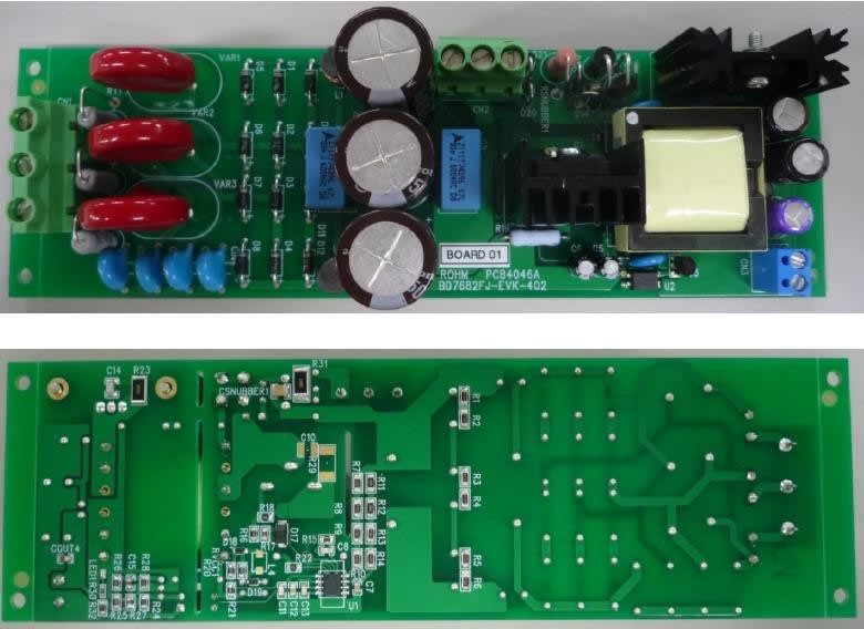
To help design projects flow more smoothly, a reference board (figure 2) is available that is ready to power up and use. it overcomes the component-selection challenges and also utilises an optimised circuit layout.
The video below shows the reference board in action.
Figure 2. The BD7682FJ quasi-resonant converter reference board which can be used with either an AC or DC input.