DSPCB - Simplified viewing of dense PCB routing.
Follow article
 Dave from DesignSpark
How do you feel about this article? Help us to provide better content for you.
Dave from DesignSpark
Thank you! Your feedback has been received.
Dave from DesignSpark
There was a problem submitting your feedback, please try again later.
Dave from DesignSpark
What do you think of this article?
Note: to use the below features, you will need DesignSpark PCB with an Engineer subscription.
To aid track routing, DSPCB feature allows nets to be selectively displayed 'by side'. It is particularly useful when increased component density on the PCB is required with surface mount components applied to both the top and bottom of the PCB. This complements other DSPCB features such as:
- “Lowlight inactive layers” i.e., the working layer is prominent.
- “Reverse view” to work as if viewing from the bottom copper side.
- “Layer’s tab” to select only the required layers.
- "Component bin", keep components off-board until required.
Here we now explore the new feature for routing a PCB using "selectively displayed by side" using the following example schematic.
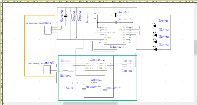
All components are surface-mount devices except the two header connectors shown in the orange box.
For this design, we decided to place the SMD's shown in the green box, on the bottom layer.
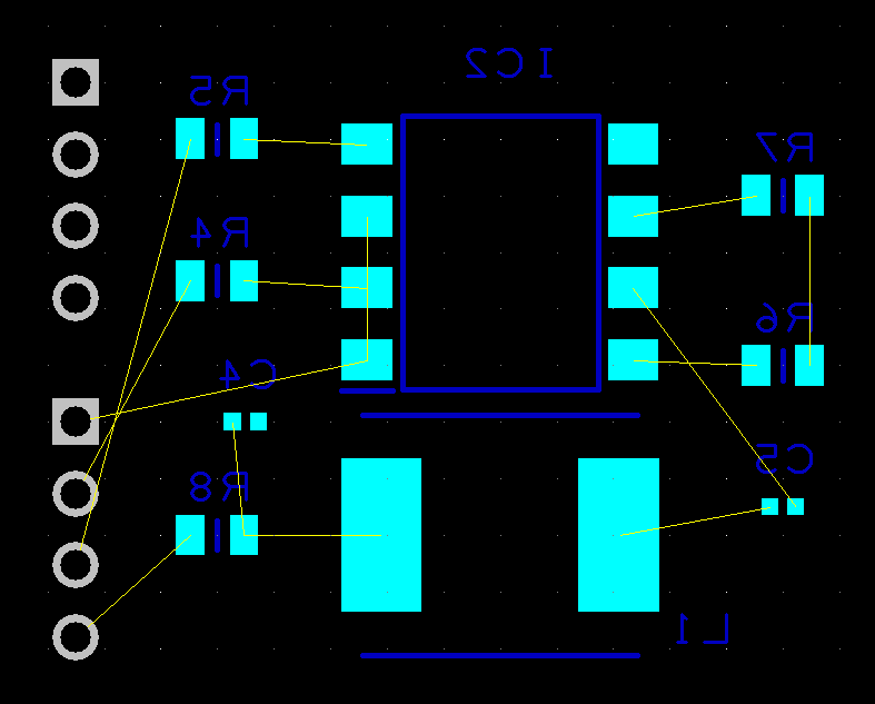
After laying out the components the default view reveals a clutter of net connections making it difficult to start routing the design.

The suggested steps are to only display the layers related to the side, so in this case, all layers not required for routing are deselected.

The above is an improvement, but the net visibility is for all layers.
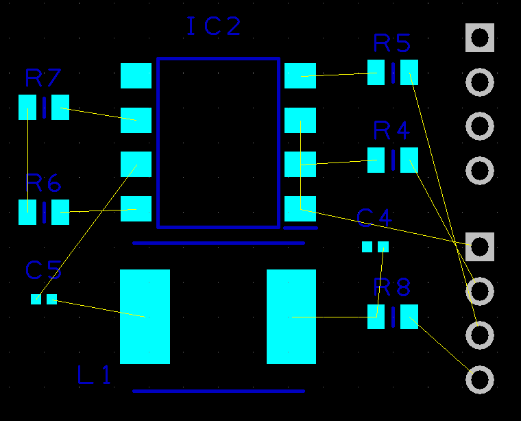
The benefit of this feature is that it allows the nets to be viewed "by side".
From "View" on the menubar, select Net Connections and you then have the options highlighted to view the Top and Bottom Sides.

Here we select "On Top Side" which provides a much clearer view to work with.

The Bottom Side can similarly be configured.
Already a feature in DSPCB Engineer is the "Reverse View" which can also aid the layout and routing by viewing from the bottom side.

Reverse View.
Conclusion.
Using this new feature "View Net Connections - By Side" removes the clutter of net lines from the other side allowing you to focus on the side of interest. This makes component placement and routing simpler. Used in combination with other routing features can speed up your layout process significantly.
Important Notes.
As user settings are recorded in the registry for ease of use of the software, if you set the "Nets by Layer" to a particular board side, this will remain set for this project when you next open this project. However, be aware it will be set in the last layers setting state for any further projects. This is setting is likely to migrate to the design project file in a later release.
Don't forget to use View - Nets "On Any Side" to complete your design and interconnect nets that change layers!
Perform the Design Rules Checks and other checks in the "Reports" to be confident that you have a successful layout.