DSPCB - BGA package manufacturing considerations.
Follow article
 Dave from DesignSpark
How do you feel about this article? Help us to provide better content for you.
Dave from DesignSpark
Thank you! Your feedback has been received.
Dave from DesignSpark
There was a problem submitting your feedback, please try again later.
Dave from DesignSpark
What do you think of this article?
Note: to use the below features, you will need DesignSpark PCB with an Engineer subscription.
With the continuous miniaturisation of components and the trend to the smaller BGA footprints, at some point, you are likely to require components with the BGA footprint in your design.
As illustrated below the footprints can vary widely, the BGA only defines the technology used to mount the component.
CR1 will not require anything special due to the pad density, but there may be 'attached' copper issues that have to be met to allow reliable solder joints.
However, U1 and particularly U2 where the pad pitch reduces, the break out of the tracks will require careful attention.
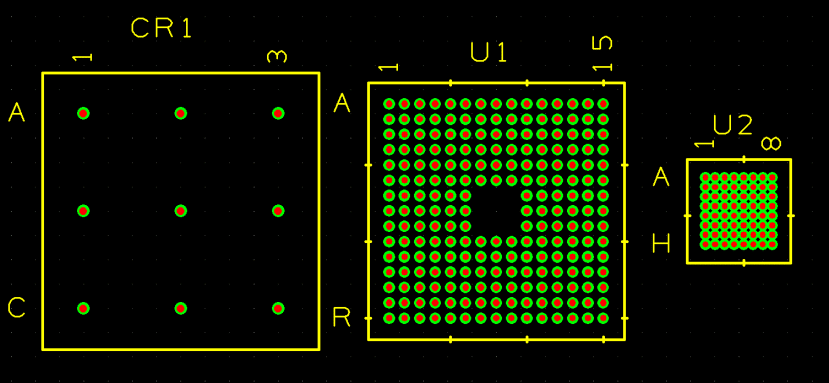
U1 and U2 will likely require a multilayer PCB and the blind and buried vias will make the breaking out of tracks easier.
Before considering the actual manufacturing requirements search the manufacturers' datasheets for suggested layouts of tracks and via placement, they may have done the difficult work for you!
Here we examine the manufacturing implications and requirements.
Starting the discussions with the free DSPCB, this offers through-hole "all layer" vias. These are the lowest cost for manufacture if they meet your requirements.
The limitation with free DSPCB (Explorer) is that the vias are of "all layer" type and will restrict track routing options on every layer. This is where the advanced blind and buried vias come to the rescue.
Blind and buried vias have manufacturing constraints.
You cannot just start adding blind and buried vias that span any layers, the manufacturing processes introduce constraints as to what is possible to produce.
There may also be additional costs incurred with inappropriate selections, so do read all of your preferred manufacturers documentation and advice BEFORE starting your PCB design. To start, let's be clear as to what blind and buried vias are:
- Blind Vias connect an outer layer to one or more inner layers.
- Buried Vias connects two or more inner layers.
- In both cases, the via must span an even number of layers.
From the description, it is obvious that these vias have special manufacturing requirements with layers being drilled at various stages during the board manufacturer, hence most manufacturers warn there will be a significant extra cost, so if you can manage with a through-hole via that will be the economical solution.
We will now consider a simple 4 layer board.
To manufacture, this will usually consist of a central core of thin FR4 double-sided board which will be etched with the inner track layers.
It will then be coated with a "Prepreg" layer and then outer layer copper foils attached. The prepreg will be hardened by the application of pressure and heat ready for etching with the outer layer copper design.
Using this layer stack-up with a solid central core, this can be drilled and plated before the outer layers are laminated and this will create buried vias between the inner layers.
After the prepreg and the outer copper foils are applied, normal all layer through-hole pads and vias are then created.
Blind vias, if the manufacturer supports these may be produced by controlled precision depth drilling or by laser drilling as part of the above process BUT many manufacturers do not support this step!
Note. An alternative to this is referred to as the 'reverse build' and has two double-sided thin FR4 cores which are joined by the prepreg layer. This was the original method of build and some manufacturers may still support this method.
With the "Reverse build" or stack-up described above with the two FR4 layers, blind vias are supported but buried vias are not!
To enable both blind and buried vias 6 or more layers will typically be required and the manufacturer will specify between which layers the vias can be added.
A very good explanation is available here from Eurocircuits.
Reviewing online manufacturing information reveals that each manufacturer has their own recommendations and they will each use their own manufacturing methods. The key point is to select the desired manufacturer and work with them to get the best possible solution for your PCB.
BGA footprints often require blind and buried vias as the pad density increases and the components become smaller. This restricts the breaking out of tracks if only all layer vias are available.
Using DSPCB Engineer's via options you can select between various solutions discussed below.
Solutions vary from:
A via in the pad, the via can be placed centrally in the pad or offset (with the connection provided by the overlapping of the copper pad and via).
The via can also be moved slightly further from the pad such that the via is connected by a short track, this latter method is often referred to as the "dog bone" due to its appearance.


The issue with any via in a pad is the possibility of solder wicking of the BGA solder into the via hole resulting in a poor or absent component solder joint.
The via placed centrally in the pad is a special case where the via has to be filled and plated to avoid solder issues. This requires many additional process steps and also has the requirement the via must be through-hole which will obviously cause some obstruction to tracking/breaking out on all layers, but it is a reliable solution.
A good description with illustrations is available from Multi-Circuit-Boards.
With the via offset from the pad centre and the via hole outside of the BGA pad copper area a through-hole via or blind via may be a suitable option. The option of 'plugging' the via will reduce the risks of solder wicking as described by EuroCircuits.
The "dog bone" approach inherently reduces the risk of solder wicking and the blind or through-hole vias can be positioned as required. The main negative point with this solution is reduced space available on the top copper layers to break-out tracks, but this may provide a lower-cost manufacturing solution to the alternatives.
Blind and buried vias in DSPCB Engineer
Having discussed the manufacturing options we will now discuss the basics of using blind and buried vias.
First, an important point is that within DSPCB, the component footprint in the library can only consist of pads and copper shapes and cannot contain vias within the footprint. The vias must be added at the PCB design stage. This is not a limitation in practice as you will not know in advance the layer spans required of the vias until design time.
With a regular pad pattern such as with BGA footprints, the easiest way to position the required vias is to set the screen grid to match the BGA pitch and the "snap to grid" to half or a quarter of the grid, vias can then be placed with ease.
In the PCB design the blind and buried vias are defined for their layer spans in the Design Technology in the "Layer Spans" tab. Once defined they will be added as selected when routing and changing the layer. It is as simple as that at the implementation stage.
A brief overview is provided here, however, this article is for illustrative purposes only.
You must as has been emphasised above contact your manufacturer to appreciate what can be produced and the cost implications.