PCB Pitfalls
Follow articleHow do you feel about this article? Help us to provide better content for you.
Thank you! Your feedback has been received.
There was a problem submitting your feedback, please try again later.
What do you think of this article?
Here are some of the errors we see that cause manufacture delays or worse.
Missing layers:
Most manufacturers need Gerber files to manufacture and these are easily generated in DesignSpark.
Using the Output tab, choose Manufacturing plots, choose Gerber and run.
Be mindful when sending files to your manufacturer. We need them all to have the full picture. The types of errors we see are
1) The files are just missing.
2) The file has no date.
If files are missing we have to wait until you send them, thus delaying your build and your project.
Gerber File extensions needed for manufacture are:
|
Layer |
File ext in DesignSpark |
|
Top |
.GBR |
|
Inner |
.GBR |
|
Bottom |
.GBR |
|
Top Mask |
.GBR |
|
Bottom Mask |
.GBR |
|
Top Silk |
.GBR |
|
Bottom Silk |
.GBR |
|
Top Paste |
.GBR |
|
Bottom Paste |
.GBR |
|
Board Outline |
.GBR |
|
Drill |
.DRL |
Drill Format
Another common error, is not providing the drill format provided in or with the drill file. This setting is provided within the Gerber Outputs in DesignSpark.
Here is an example of what this information looks like:

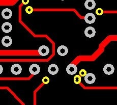
Overlapping Drills:

Solder Resist Pads:

Another pad complaint is extra pads. This can happen when the designer uses the same components in different layouts and imports the solder resist for the component. Due to the different layouts extra pads may be placed in the layout which can cause exposed traces, plains etc.
These errors are not found at Design For Manufacture (DFM) checks and could make it to the final PCB. This might affect the functionality of the PCB.
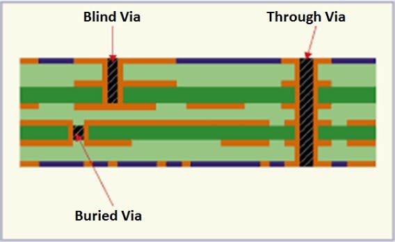
Avoid Via-In-Pad
Often components packages such as BGAs & QFNs are designed using via in pads. The trick in prototyping is to try and avoid them if at all possible. Via in pads can pull the solder away from the component to the other side of the via. So the smaller components may not have a solder connection, the larger ones may have a bad connection and the balls on BGA may simply disappear.
If you really need the via in pad, make it as small as possible to reduce the pull, cover them with solder mask*. Another note of caution, air can get trapped if the other side of the via is capped by solder mask. The air will be ejected during the soldering process. The air can affect the solder and result in bad joints.
*Be sure to tell your manufacturer that you want the vias masked as often they remove that mask unless it’s requested.
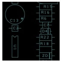
Provide Readable Documentation with Good Silk-Screening

It is important to properly mark components with polarity. For ICs, pin 1 and orientation is crucial to specify.
Calling all DesignSpark users, please tell us about your experiences and any pitfalls. Tweet us at @MintTekCircuits or @DesignSparkRS, or email me directly at siobhan@mint-tek.com. As a regular blogger, I’m always looking for key learnings to share with my audience.
At Mint Tek Circuits we use a global panel of proven PCB manufacturers to get the best technology, at the best price, in the best time. We work closely with the DesignSpark community to create a simple supply chain for design engineers.
Experience our online PCB Quote Calculator for yourself


