How can I pour copper?
Follow tutorial
 Dave from DesignSpark
How do you feel about this tutorial? Help us to provide better content for you.
Dave from DesignSpark
Thank you! Your feedback has been received.
Dave from DesignSpark
There was a problem submitting your feedback, please try again later.
Dave from DesignSpark
What do you think of this tutorial?
This tutorial requires:
DesignSpark PCB V11.0.0Copper Pour is used to flood areas of a PCB layout with copper, usually connected to a nominated signal through ‘thermal’ connections, typically Ground (0V) or +5V. This facility will then create voids around tracks, component pads, vias and other electrical obstacles.
For this we have the Add Copper Pour Area and Pour Copper options.
If a copper area is to be inserted without the need for voids around unconnected tracks, components or pads, the Add Copper option can be used.
The principle of this facility is to insert a Copper Pour Area and ‘pour’ the copper into this area.
1. To create a copper pour area
From the Add menu, select Copper Pour Area > then Rectangle. Other Pour Area options are available for adding different shapes. In our example below we will add the pour area to the Top Copper layer. Pour areas and poured copper can be added to any electrical layer. To change layers, select the pour area and click <L> followed by <Enter> as we did when editing tracks.
The shape can be created on the design and the pour area can be drawn protruding outside the board outline. DesignSpark PCB will pour the copper using the Spacing rules and rules defined for the Pour area.
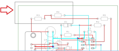
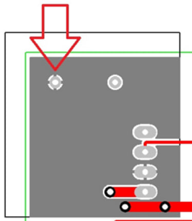
Following our example below, draw a basic rectangle pour area shape, this is shown in black in the top left hand side of the design:
For this example you will see how easy it is to add a poured copper area.
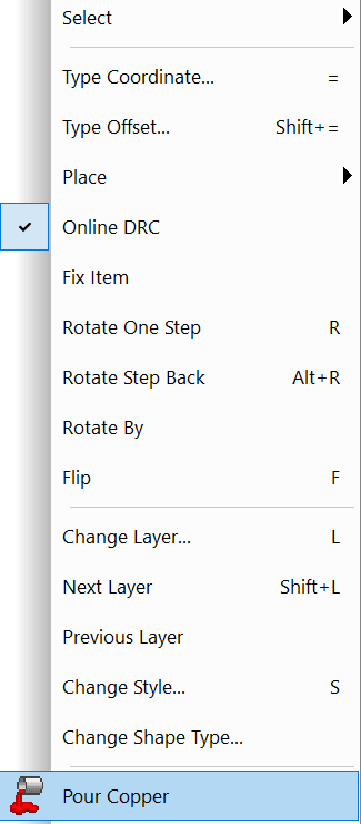
Right click on the pour area.
From the shortcut menu select Pour Copper.
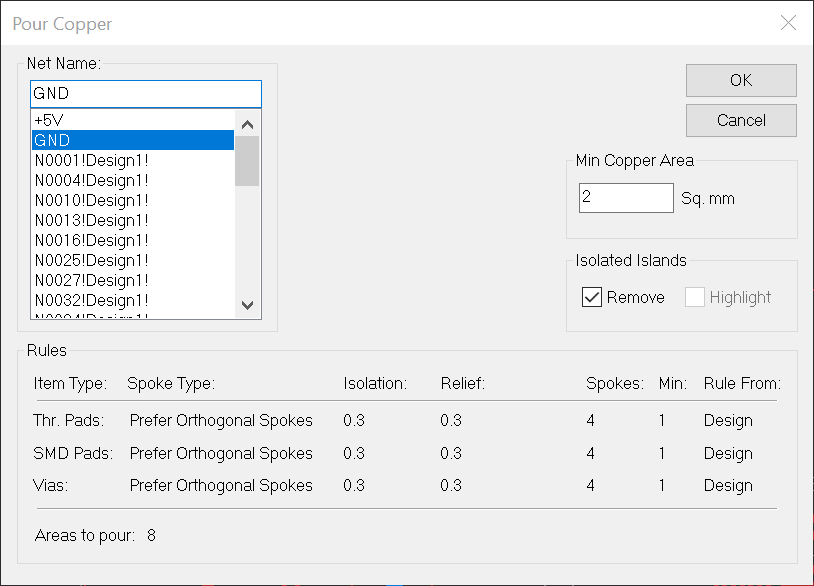
A dialog box is displayed from where you can select parameters for the poured area, such as the net name association and thermal relief/isolation spaces.
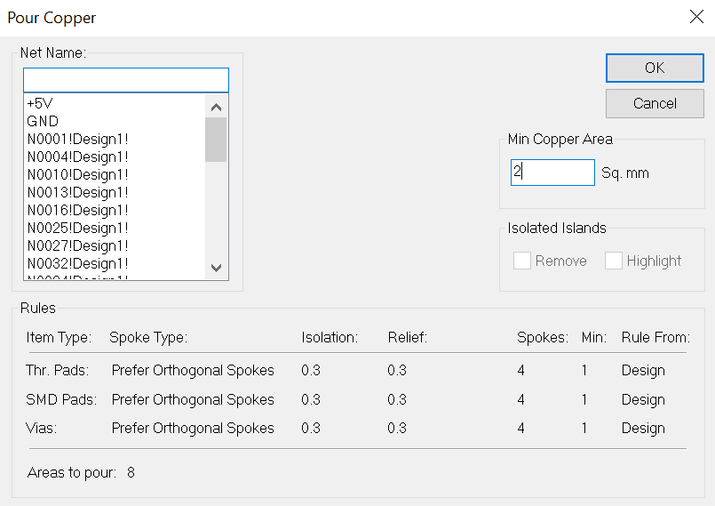
For this exercise, leave the Net Name blank and simply click OK.
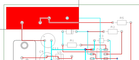
Notice that the poured copper has obeyed the Spacing rules of all defined items to copper including Board to Shape rules.
2. Making the copper pour area intelligent
There are more facets to the poured copper than we have discussed above. The poured copper can also have a net name associated with it so that when poured, pads are connected via thermal spokes to the copper itself. To do this, select the pour area and from the shortcut menu select Add To Net. Select the net name required from the list and then re-pour the copper. Try it again using GND as the net name and click OK.
The Copper Pour Area line will not appear on your manufactured boards, they provide the system with an intelligent area into which the copper can be poured. During the pour of an area, all spacings are used as defined in the Spacings dialog. To edit a copper area shape, it is recommended that the poured copper be unpoured first using Clear Copper (right-click the poured area for this option). The Copper Pour Area outline can then be edited and re-poured.
When no specific pour areas are selected, using Pour Copper from the shortcut menu will pour (or re-pour) all areas in the design. To ensure that they are poured in the correct order (important if they overlap), use the Copper Area Properties (Edit menu -> Properties) and set the Order field (lower numbered areas are poured first).
Warning: Do not pour copper onto layers which have been defined in the Layers dialog as Power plane. When plotted this can cause strange and unrequired results. See Split Power Planes in the built-in help documentation if this is what you are trying to do.
Here are some of the other options available in the Pour Copper dialog:-
Isolated Islands: Isolated islands of poured copper are created when some of the poured copper pieces do not connect to any other items on the net. Use this section to decide what to do with these islands.
Remove - Use this to automatically remove isolated islands after pouring.
Highlight - Use this option to keep the islands but highlight them for you to easily delete them interactively after the copper has been poured.
Rules: The rules for copper pouring control the appearance of the thermal relief on pads and vias attached to the net you are pouring and can be set in two places. The overall copper pour rules are set in the Design Technology -> Rules. If you wish to override these settings on an individual area, you can do so by selecting the area, and right clicking, select Properties and click on the Area Tab.
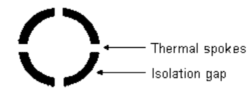
Spoke Type - shows how the pad or via will be connected to the poured copper.
Relief - This shows the width to be used for the thermal relief spokes.
Isolation - Shows the isolation gap, also known as the thermal break, to be used between a thermal pad and the poured copper.
Spokes - shows the required number of spokes added for each pad and via.
Min - shows how many spokes need to be added for to avoid a pour warning.
Rule From - states whether the rule came from the design level rules, or from an area override.
3. Reporting Issues and DRC errors
If any issues are found while pouring, for example if there isn't enough room to legally insert as many thermal spokes as are required by the design rules, then these issues are listed in a report which includes links you can click on to access those locations in the design.
In addition, these issues are marked with a Design Rule Check error using the error code "Cu" so that you can find them using the GoTo Bar. The error markers within a copper area are cleared before clearing or re-pouring that area, or you can delete them yourself as you work through them resolving the problems.