How can I create an LCD module as a component?
Follow tutorial
 Dave from DesignSpark
How do you feel about this tutorial? Help us to provide better content for you.
Dave from DesignSpark
Thank you! Your feedback has been received.
Dave from DesignSpark
There was a problem submitting your feedback, please try again later.
Dave from DesignSpark
What do you think of this tutorial?
This tutorial requires:
DesignSpark PCB V11.0.0This tutorial shows a complete step-by-step procedure to create an LCD module for use as a component. Although this is an LCD module the techniques can be equally applied to microcontroller, RF, I/O modules as required.
A quick search will identify many different LCD modules available for character and graphic displays incorporating the main IC and display integrated onto a compact PCB display module ready for use.
How can these modules be used within DesignSpark PCB as components that will form part of the final design?
These displays modules provide 4 mounting holes and a PCB connector as the interface. They can therefore be treated as a simple connector with four spaced mounting holes, plus for convenience of assembly within an enclosure can indicate the position of the LCD window.
Essential steps in this process are to identify the correct mechanical drawing for the many LCD module configurations. Even similar ones may vary slightly between manufacturer, but some have significantly different footprints.
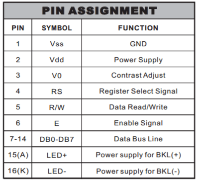
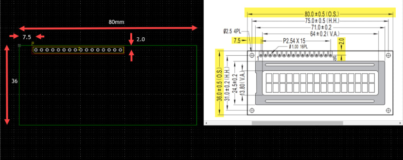
This shows RS 125-329 16-character 2 row module with an SIL 16 pin connector. The connector from other manufacturers may be in a totally different locations showing that it is essential to consult the mechanical diagram.

The following for example shows the RS 214-3525 16x02 from Powertip with a 8x2 DIL header connector.

Create the component.
For the purposes of this example, we shall create a component in DesignSpark PCB for the "Fordata"
RS part: (012-5329). First, we identify the key dimensions:

We require the connector pad hole locations and also the mounting hole locations in relation to the module board dimensions as highlighted above.
Note. Unless otherwise indicated a dimension is assumed to be symmetrical about a horizontal or vertical centre line.
Step 1. Create the schematic symbol.
The symbol will consist of 16 pins as defined below.
Launch the Library Manager, select the 'Schematic Symbols' tab and click the 'Wizard' button.

Step through the configuring steps leaving everything at their default values.
Select a connector as the "..kind of symbol.." (NOTE if you were designing an 8x2 connector for the LCD type you may wish to consider a 'rectangle' symbol, but it is purely your choice for ease of visualisation).
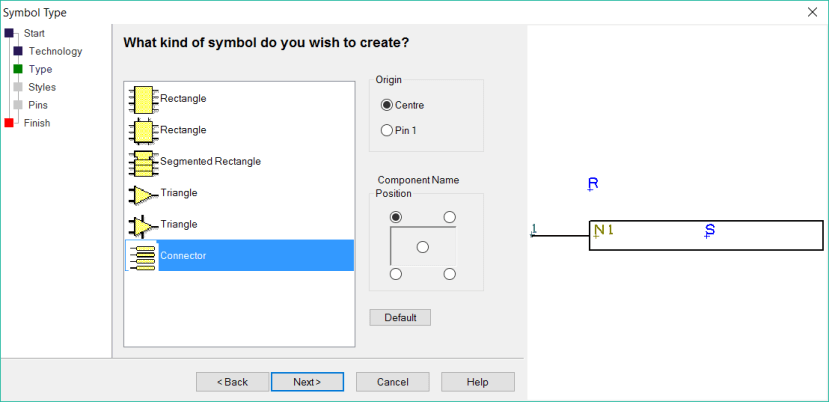
Then at "Specify the pins required..." select 16. The other dimensions shown are for the schematic symbol, leave these at their defaults.

Finally name the symbol for ease of identification or your local standards.
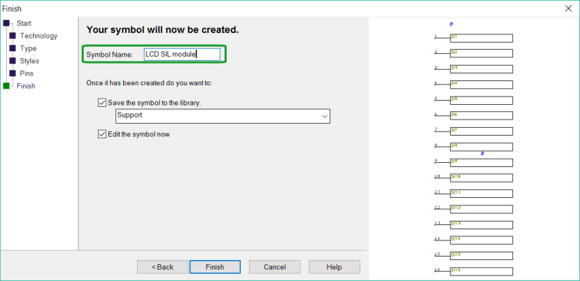
Leave the check boxes ticked to save the symbol and select from the pulldown menu the library location where the symbol will be saved.
Also leave the check box ticked to 'edit the symbol now' which will launch the symbol editor with the symbol.

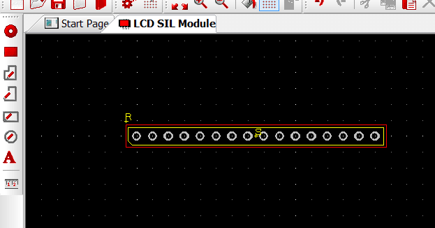
The above is the basic symbol i.e., just the connections and we can now edit it to appear as we wish to see it on our schematic sheet.
You can make this as elaborate as required using the simple shapes and text option provided. Here is our symbol which just symbolically shows a matrix, it can be edited further to show 16x2 characters or just have a text description.

Step 2. Create the PCB symbol.
This is more demanding in that it must be dimensionally accurate. Here we show some techniques on how to use some of the features to make this as easy as possible.
Launch the Library Manager, select the 'PCB Symbols' tab and click the 'Wizard' button.
Step through each window and make selections as appropriate. The key windows are detailed below.
As the datasheet is in ‘mm’ we select a metric technology file.

The SIP footprint is most appropriate for our requirements.

Next, we specify the number of pins, pitch, hole size and pad width.

The Hole Diameter has been selected to match the LCD module in this example.
Step through and save and name the PCB footprint. This requires further editing for our LCD module so tick the check box to launch the footprint editor now.

In the editor we now have the basis for our LCD with just the connections.
Now we will add the module outline.
Add an outline as a rectangle shape on the documentation layer that simply encloses the connector. Next select the top edge and position that 2mm above the centre of the pad hole. In this case it can be simply achieved with using the grid, but all dimensions can be checked with the measure tool as shown.
Now we will add the module outline.>
Add an outline as a rectangle shape on the documentation layer that simply encloses the connector. Next select the top edge and position that 2mm above the centre of the pad hole. In this case it can be simply achieved with using the grid, but all dimensions can be checked with the measure tool as shown.>

Next, we position the remaining edges.
For example, select the lower board edge and press the shortcut key '=' to display the current coordinates from the Relative Origin, type in the required new vertical dimension, click 'OK' at it will be precisely set.

Repeat for all edges setting the relative origin and a reference point and using the shortcut '=' for the selected line update its 'X' or 'Y' dimension as appropriate.
We now have the board outline positioned correctly relative to the connector.
We now add the mounting holes which are 2.5mm diameter and 2.5mm in from each board edge at the corners. We wish to place these as circles on the documentation layer, however it is simpler to place these as a pad, convert to a shape and move to the documentation layer as shown.
(Note: circle position when used as a shape is defined from the circumference, hence the pad is a better solution in this instance).
Set the Relative Origin at a corner if it is not in the required location, zoom in and with the cursor at the required position press the shortcut key 'O'. You may alternatively select the left vertical board edge and from the right click menu select Origins--> Set relative origin at item.

NOTE. The relative origin of a line is at one end, so select either of the intersecting board outlines that provides the origin in the desired position.
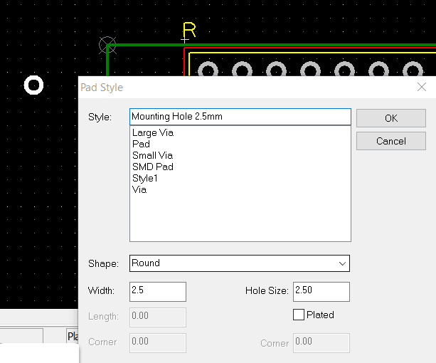
Now place the mounting holes which are pads without copper.
Select the Pad icon, Press the shortcut key 'S' to change the Pad Style. Name the hole with a descriptive name such as 'mounting hole 2.5mm' and set the values as required, here we have the settings for a simple hole, click OK and accept and close any warnings.
With the newly dimensioned mounting hole selected on the component press the short cut key '=' to easily position. Ensure the relative check box is selected and edit the position values for the required location. Press 'OK' to place.

Repeat for the other positions and your basic LCD footprint is complete.
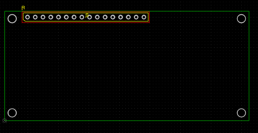
Finally move all these holes to the documentation layer (otherwise the holes will remain as component pads).
Click each pad in turn to select and from the right click options change the pad type to a shape.

Then change the layer to 'Documentation' using the 'Change Layer' option or the shortcut 'L'.

repeat for the four mounting holes and save the footprint.
You are now ready to create the component.
Step 3. Create the LCD component.
In the Library Manager open the 'Components' tab and click the 'Wizard' button. Step through the wizard completing each form.
Select a 'normal' component, this will have a schematic and footprint symbol.
Complete the component details window.
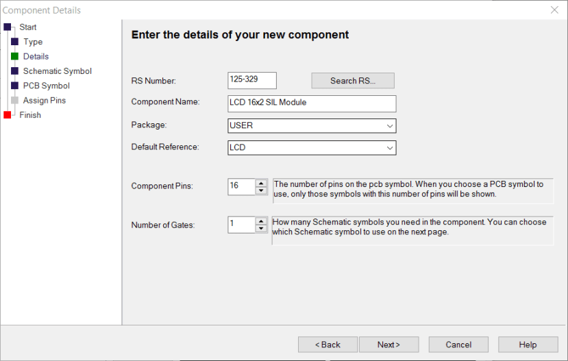
Add the part number used by the BOM, a descriptive component name to easily identify in the library, define the package as 'User' as it is nonstandard and select or provide a reference designator.
Define the part as 16 pins and the number of gates as one as there are no duplicate entities.
We next select our schematic component from the list which will be all symbols that match the pin count from the selected library. Locate your schematic symbol in the library.
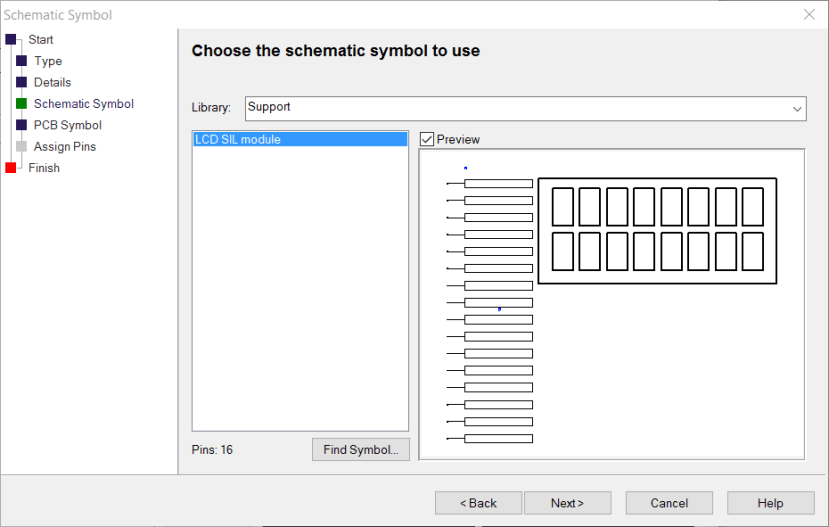
Then we select the appropriate PCB symbol.

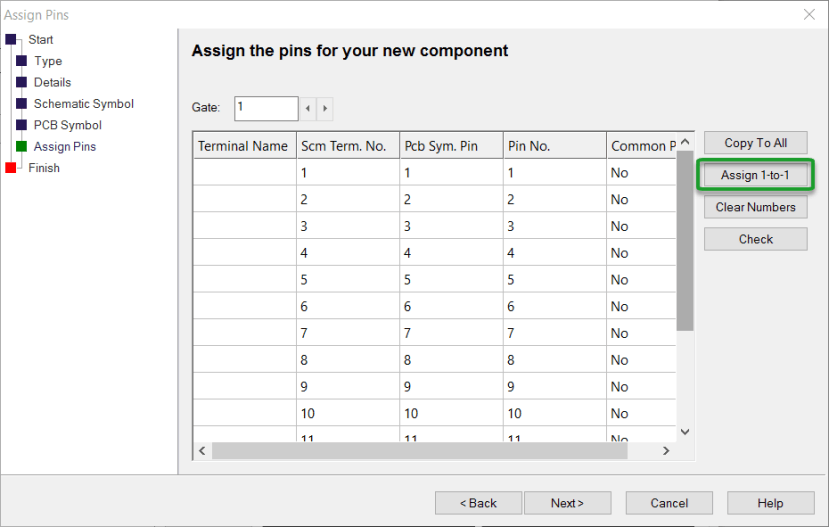
Now the symbols are brought together by mapping the schematic symbol pins to the footprint pins, click the 'Assign 1:1' for this part.
and finally click the 'Finish' button with the check boxes ticked.
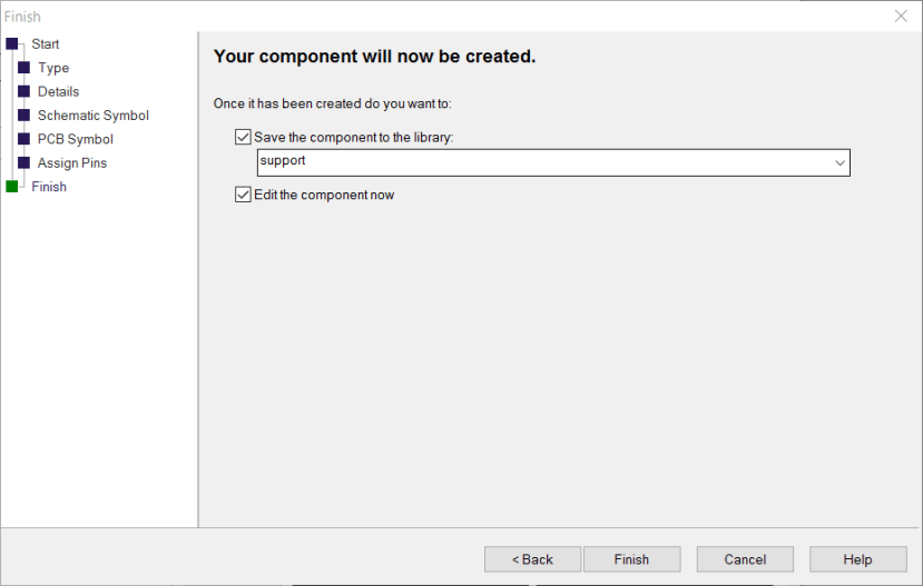
In the component editor that opens we can assign pin names.

Now save the component and it is ready to use from the library in your schematic and PCB designs.
Further improvements to both the schematic and PCB symbols can be made as required, such as having a true 16x2 character layout for the schematic and adding the actual positions of the LCD characters on the PCB footprint as may be required to align with an enclosure cut-out.