How can I convert schematics to PCB?
Follow tutorial
 Dave from DesignSpark
How do you feel about this tutorial? Help us to provide better content for you.
Dave from DesignSpark
Thank you! Your feedback has been received.
Dave from DesignSpark
There was a problem submitting your feedback, please try again later.
Dave from DesignSpark
What do you think of this tutorial?
This tutorial requires:
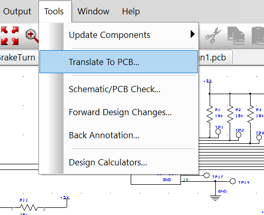
DesignSpark PCB V11.0.0If you have created a Schematic in DesignSpark PCB, the final process before starting on the PCB design itself is to translate the Schematic design into the PCB design editor.
When you are in a position where you wish to go ahead with this translation you should select Translate To PCB from the Tools menu and use the Translate To PCB option.
This will display the New PCB wizard. Whether you create a PCB design by using the Translate To PCB option or by using the New option and PCB Design, you will be presented with the New PCB Design Wizard.
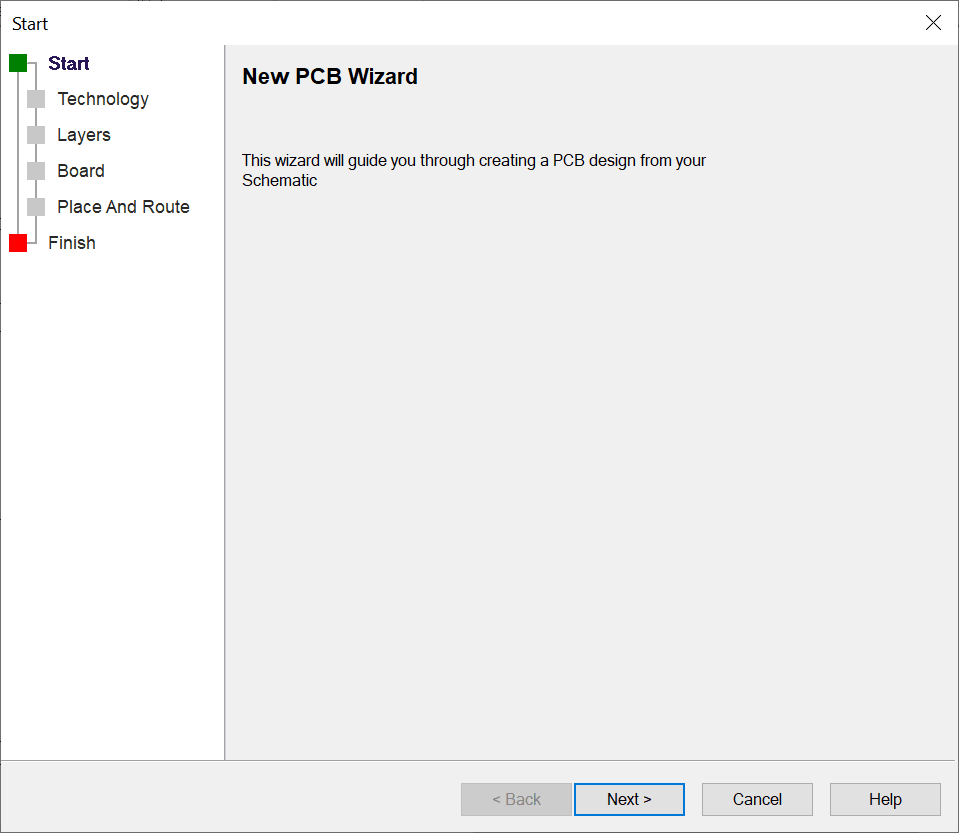
The New PCB Wizard
This wizard presents you with a set of dialog boxes which will take you through a sequence to define aspects of your design in the PCB design editor. Help is available for each page by pressing the <F1> key at any time.
Click Next > to move onto the next page. You can also click the page name you require in the list at the top left-hand side but we recommend you to work through the wizard pages in sequence.
On the Start page check the box to agree with the disclaimer. You must click this to proceed further. It is only shown once after you have selected it for the first time. Click Next > to proceed.
The Technology page allows you to predefine a Technology file and your design Units. Technology files allow you to create a set of sizes (styles) and design spacing rules that can be used time and time again on different designs. This enables you to be consistent with naming conventions and standards. It also provides you with a fast way to get your designs started.
The Units are defined here to get you started, as are the unit Precision, but both can be changed at any time during the design process.
For our example, select Choose Technology File: (we want to use an existing one), and select Double Sided (Metric) from the drop down list.
For Units: choose mm and 3 as the precision.
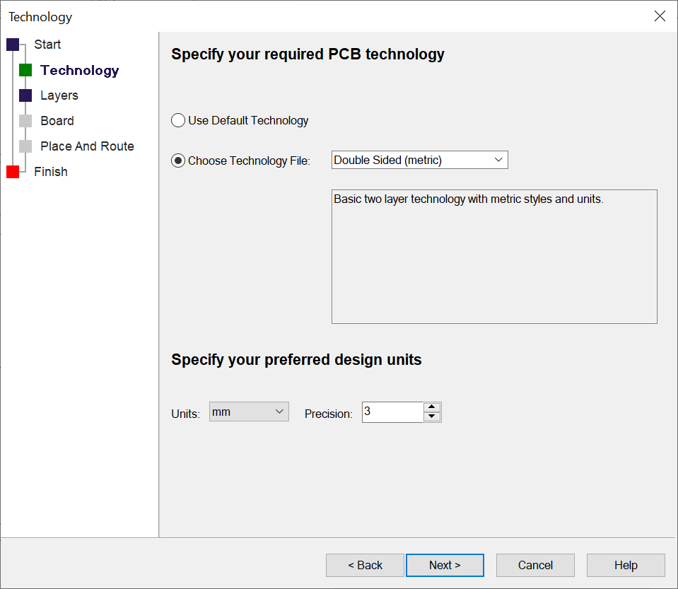
Click Next > to proceed.
The Layers page allows you to change the layer usage from that of the Technology file if you have specified one. For our example, we will leave the selection as Use Layers From Chosen Technology File. The layers selection will display the contents of the Technology File but you cannot edit them, only view them. These can be changed once in the PCB design anyway, this dialog gives you visibility of the selection and the ability to make changes upfront.
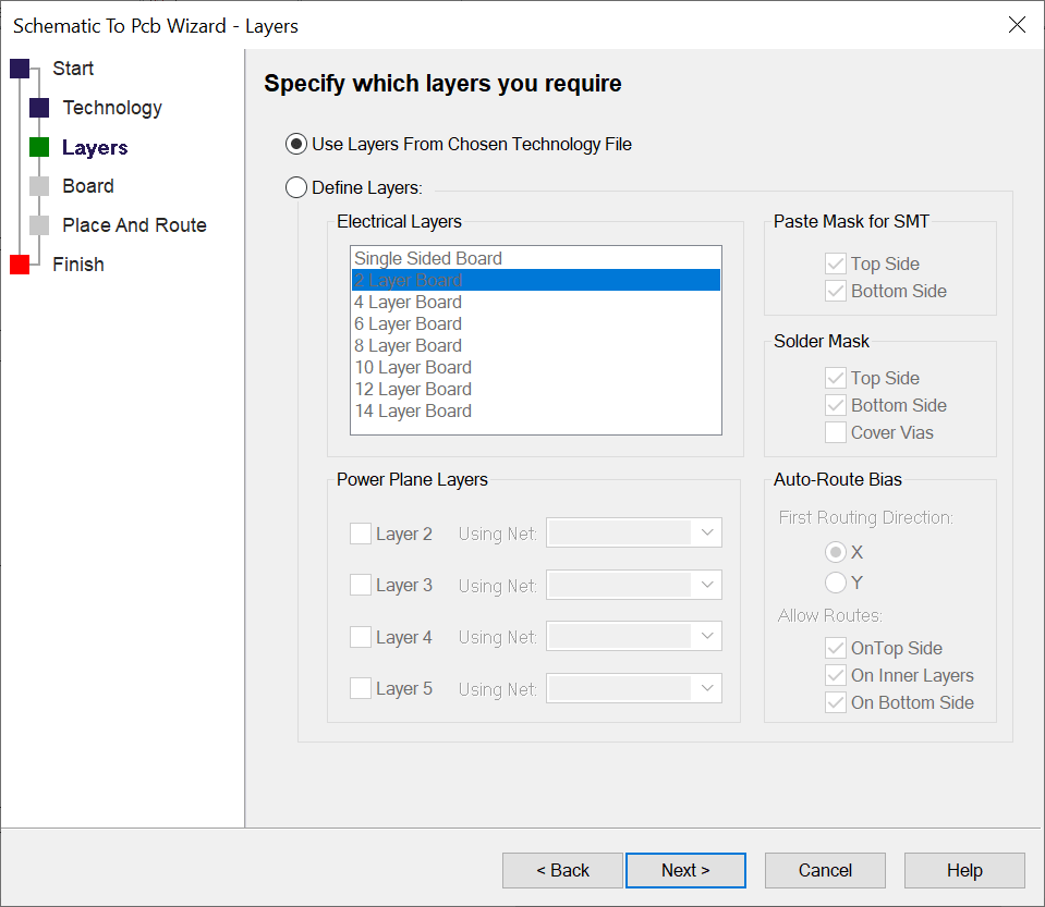
If you decide to make changes to the Layers, the Define Layers button should be selected. Use this once you understand the implications of making changes to layers. Leave the selection as Use Layers From Chosen Technology File.
Click Next > to proceed.
You should now define the shape and size of the board outline using the Board page. You can define your board as a rectangle/square, or a circle and its Width/Height or diameter in the current units.
If your chosen Technology file contains a board outline (which it can), you can elect to use this.
You can also choose to Copy Board Outline From Another File (another PCB design file or different Technology file). If using a PCB design for the board outline, the PCB file must reside in the Technology file folder.
For our example, choose Define Board Size and set the Width and Height to 76.2 each.
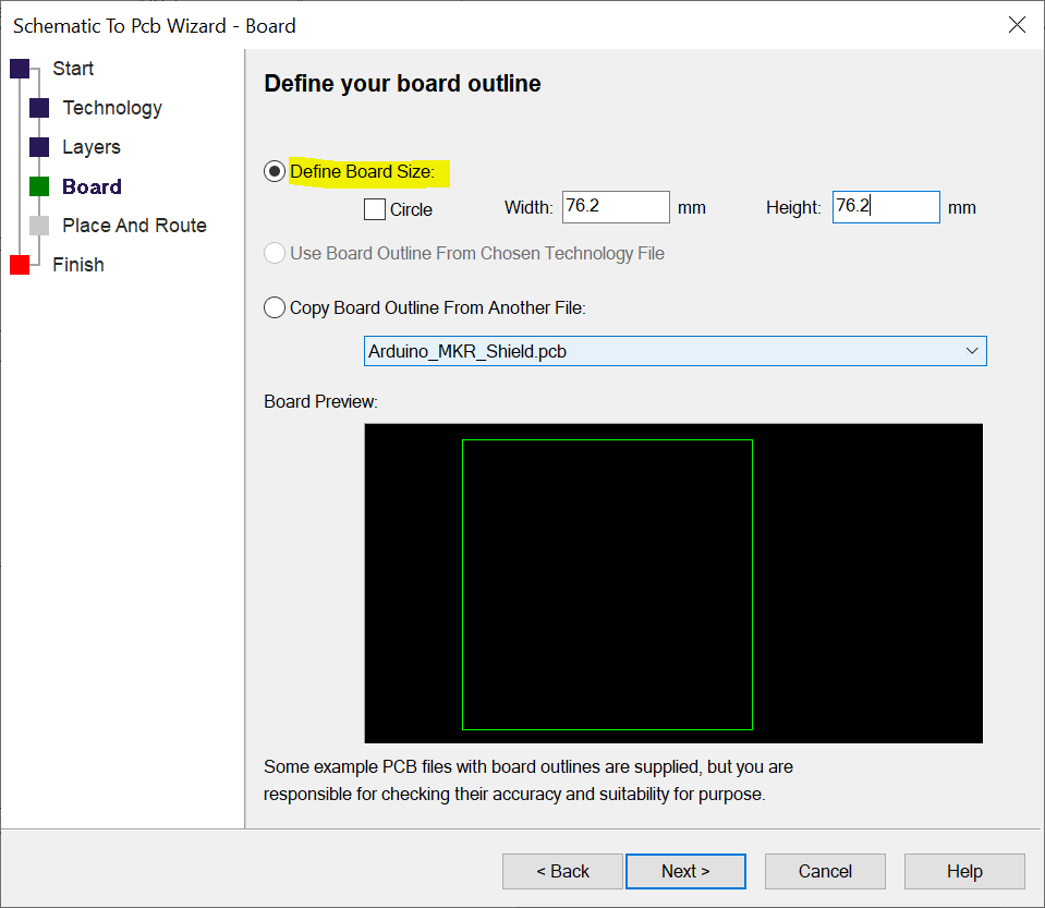
Click Next > to proceed.
The Place And Route page allows you to automatically let DesignSpark PCB place components and then route their connections using the auto router.
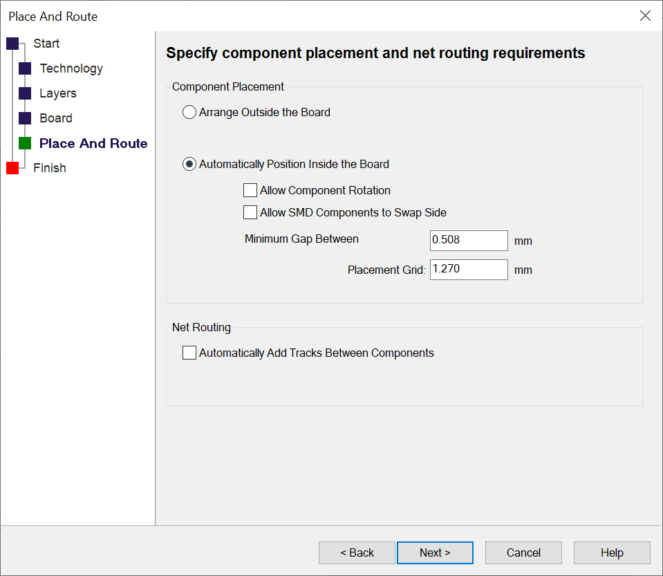
Under Component Placement, you can elect to place components in an Arrangement Outside the Board to stack them by type outside the board outline. This makes them easier to see and place manually.
Use Automatically Position Inside the Board to place the components on the board. It will attempt to work out the best way to arrange the components on the board to keep the total length of tracks as small as possible, without packing them too tightly together. The two controls will enable you to define how components are placed using your preference and possibly, your assembly or manufacturing processes.
For our example, change the Minimum Gap Between Components and Placement Grid values to 2.54 (mm) each. We will allow plenty of space between the components. If you decide you’d like less space between each component, you can run the Auto Place Components > option from the Tools menu once in the PCB editor, you don’t need to go back through the New PCB Wizard. Before the design is routed, this can be an iterative process of trial and error.
Don’t forget also, even though the Auto Place option has made your placement for you, you can manually place components at any time to refine the placement by picking and dragging them (more of this later on).
Check the Automatically Add Tracks Between Components box to let the router convert the schematic netlist into PCB tracks. This is only available if you have chosen to auto place the components in the section above. Leave unchecked if you intend routing the board by hand, or need to alter the design before letting the auto router finish it. You can run this option once in the PCB Design using the Auto Route Nets > option from the Tools menu.
For our example, check this box to let the auto router route the design for you (you can unroute it if you decide to have a go with the manual routing options).
Click Next > to proceed.
Use the Finish page to set your PCB Design Name and to Save it to a file. By default, the PCB design name will be the same as the Schematic design name. It doesn’t have to be but it makes sense to keep them the same, especially when running options such as Forward Design Changes which will look for the opposite design type of the same name.
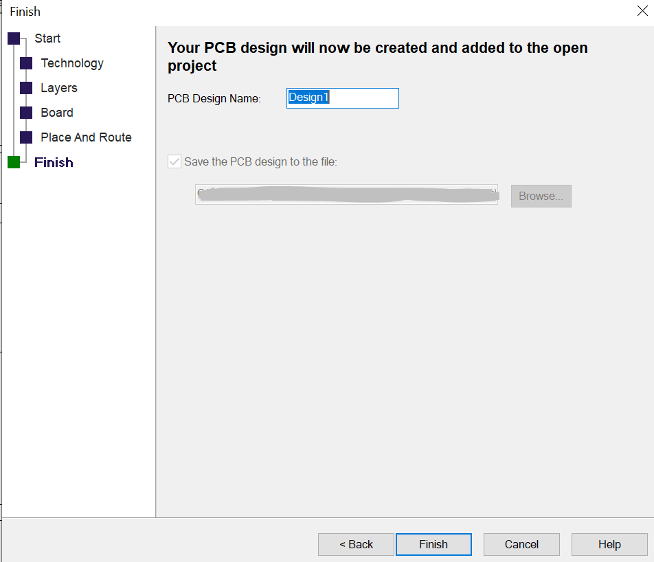
At any time (and before you hit the Finish button) you can go back to one of the previous pages by selecting the page name from the list displayed.
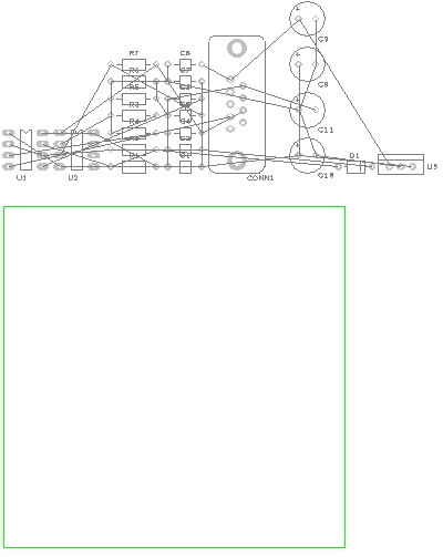
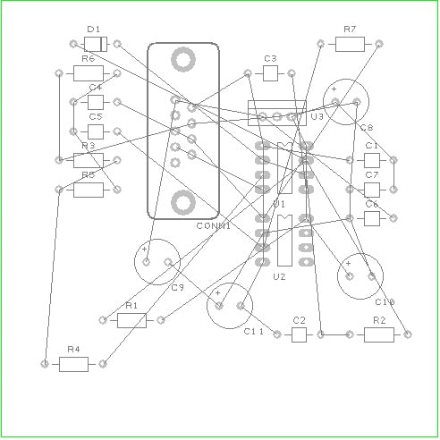
When you click the Finish button, the PCB design editor will run up and your PCB design will be ready for use. Your design background will be black, we’ve changed the colours for the picture so it is easier to view in the PDF file.
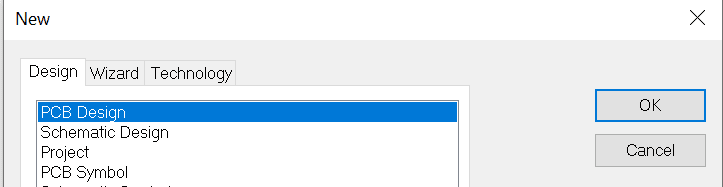
Starting a New PCB Design without a Schematic
If you intend to start a new PCB design without using a Schematic design first, select New from the File menu and select the PCB Design option.