How can I perform a Design Rules Check (DRC) on my PCB layout?
Follow tutorial
 Dave from DesignSpark
How do you feel about this tutorial? Help us to provide better content for you.
Dave from DesignSpark
Thank you! Your feedback has been received.
Dave from DesignSpark
There was a problem submitting your feedback, please try again later.
Dave from DesignSpark
What do you think of this tutorial?
This tutorial requires:
DesignSpark PCB V11.0.0DesignSpark PCB contains a Design Rules Check (DRC) function available from Tools --> Design Rules Check or the icon on the tool bar.

The parameters checked on the PCB are compared with your Design Technology parameters.
The DRC window contains many options for you to select individually or in groups to improve and optimise your design as shown:
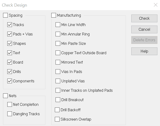
It is advisable to work through these to ensure the greatest success with your manufactured PCB, however selecting all options at one time may cause confusion if you have many reported errors.
The PCB below is an example to show some errors using the above settings.
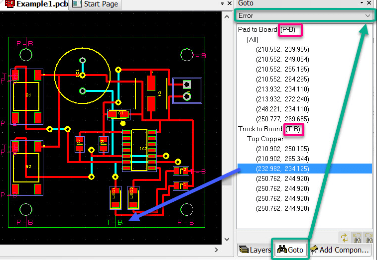
It is recommended that you have the Interaction Bar active for correcting errors.
Launch the Interaction Bar via the short cut F9, then along the bottom select the “Goto” tab and from the pull-down menu select “Error”. When you run the Design Rules Check using the “Check” button, all the errors found will be listed. Notepad will also open providing a list of the errors and the PCB will be updated with the error markers identifying the type of error and a marker line to show the location of the (first found) error. Note that there may be multiple errors from the same object that need resolving such as the holes shown above from each edge of the board outline.
Selecting an error from the list will highlight the error on the PCB as shown to make the issue easier to resolve.
In the above example, the PCB outline was made smaller to cause the errors shown. It easy to believe that the spacings are much larger than reality when working on a large scale! The holes in this PCB for example are clearance for a 2.5mm (0.1”) pillar.
In this instance the PCB outline and holes are restored to that shown below which results in no errors for the selected ‘checks’. When you recheck your Design Rules, you will normally “Delete Errors” before performing the “Check” to see that the errors are removed.
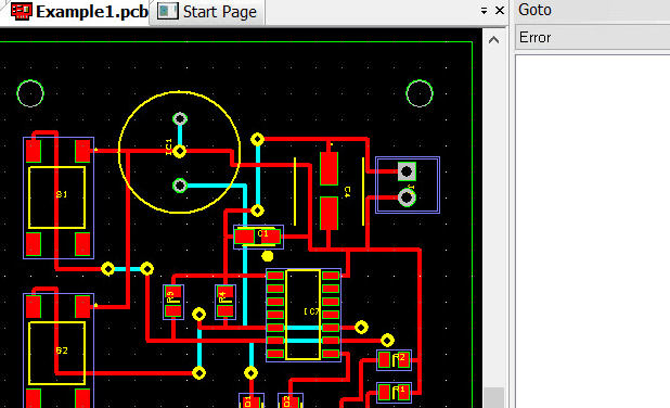
In your design where the PCB outline may be fixed you will need to reposition components and tracks to achieve the required result.
Continuing with the checking you may gradually add additional items to check. Below is the result with all the checks enabled.
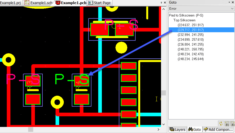
These are Pad to Silkscreen errors and need to be resolved as silkscreen printing on a solder pad can result in soldering problems. Select each component reference such as R4 and move it outside of the pads and to a location where it can easily be seen with the component in position.
This covers a few examples of how to use the Design Rules Check function. More details are available in Help describing the types of errors.
It should also be noted that this is a “check” for issues you should examine, you may decide that the reported issue can be ignored. A typical example of this is a connector which you require to overlap the PCB outline.