Pitfalls - Why can't I?...
Follow article
 Dave from DesignSpark
How do you feel about this article? Help us to provide better content for you.
Dave from DesignSpark
Thank you! Your feedback has been received.
Dave from DesignSpark
There was a problem submitting your feedback, please try again later.
Dave from DesignSpark
What do you think of this article?
Occasionally the Support team get asked questions where a user has accidentally or intentionally changed a setting not appreciating the consequences, here we discuss the most common settings changed and their impact.
Why can't I add a net to my schematic or why aren't my nets 'connected'?
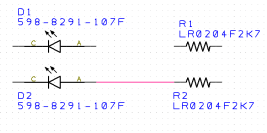
A typical schematic view is as below.

The corresponding "Colours" window accessed by the shortcut "C" is as below.
The name "Colours" is slightly misleading as some settings do affect the function.
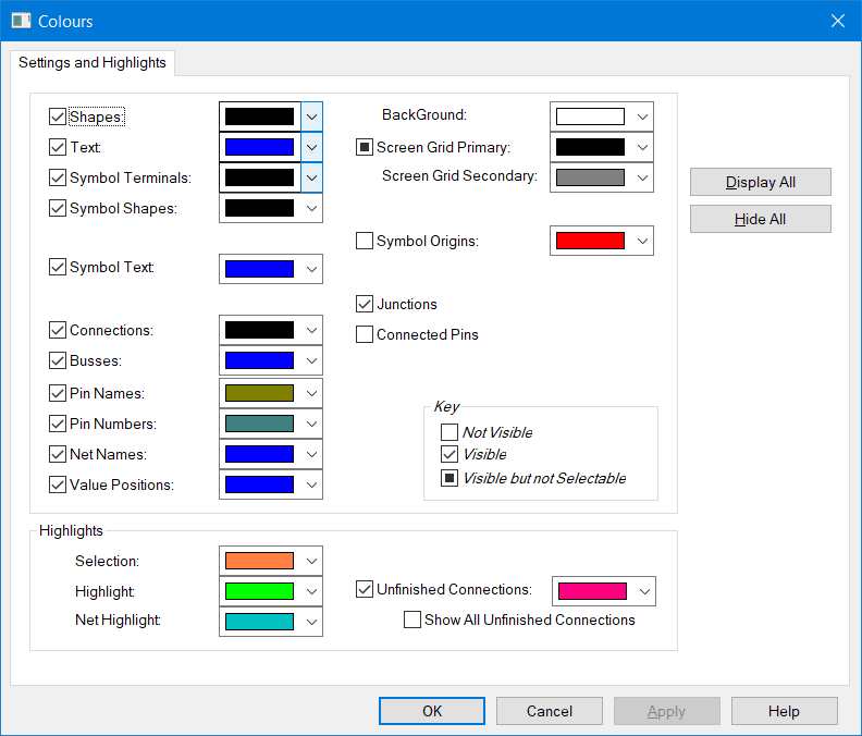
As an example, some new users decide they do not want the Symbol Terminal "X" shown and remove the associated tick.
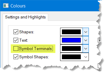
Not only does this remove the "X" but also the automatic net connection feature when trying to connect a net to the pin! Double-clicking on the end of the component symbol actually selects and highlights the symbol.
If you manually add the net it will show as an "unfinished Connection" and will not be connected to the pins. If you ever wonder if a net is correctly connected selected it and drag it away from the connection points and it will be clear if the net is connected! Use "undo" to restore back to where it was if it is correct.
What use is the Symbol Terminal option? It can be used when the schematic sheet is finished prior to printing should the "X" not be required.
PCB pitfalls....
The Colours Window also has some points to be aware of.
Why can't I select.....
In the "Layers and Layer Spans" tab there is a column headed "Selectable" in which the layers can be set to Yes or No. If you set any of these to "No" then you can't select them in the PCB edit window!
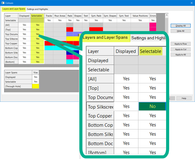
In the above case, nothing on the Silkscreen Layer can be selected and hence moved.
This is useful for preventing accidentally moving component references, logo's and general text in the final stages of a design, but don't forget to make the layer selectable should you need to move something.
Design Rules Check - "Gap is 8 needs to be 8"
Some users get an error as in the example above which appears confusing when first experienced, but it is simply down to the precision of the numbers that you have selected to display. DSPCB and Engineer subscription use a high precision internally but for display purposes, you can select the number of digits displayed after the decimal point.
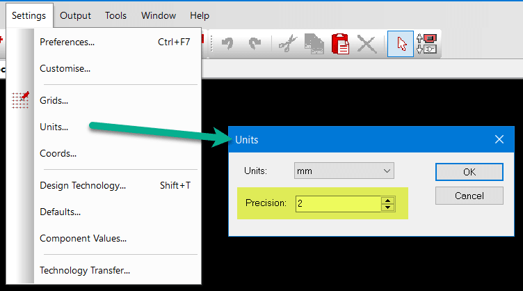
This is available as shown below from "Settings".
Below shows a precision of '2' which will display for example 2.54mm.
However, if the precision was set to '0' the displayed value would be rounded to 3
The displayed precision functions across the program, not just the reports. Below shows the Design Technology spacing values with a precision of 2 in the top image and 0 in the lower image which could obviously lead to some beginners confusion!
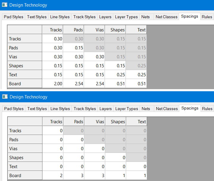
Always work in an appropriate display precision. If you see a confusing measurement displayed, increase the precision so you can clearly see what is being set or reported.
DSPCB Engineer subscription has another feature that although very useful, can cause confusion when the feature has slipped from memory!
The feature is detailed here, viewing the Net Connections by side but should you forget you have View - Net Connections - On Bottom Side selected you will not see any nets/rubber bands for connections on the top side. Ensure you have "On Any Side" selected!

SMD free pads by PCB side.
When you add a surface mount pad it will by default be on layers [All], but you are most likely to want this on a particular board side as shown below:
The 'mouse over' highlights the layer(s), as shown they are in square brackets [ ] which represent the side.
Note also the layer stack order used below, by placing the smaller paste mask opening above the copper pad and the larger solder mask opening below the copper you will see all the pad detail.

When you want to change a free pad to the other side of the board make sure you select a side in brackets [Top] or [Bottom] as this will transfer the masks as well. If you were to select Top or Bottom copper for example, only the copper changes side!

For most users this will never become an issue as the pads are part of the footprint of a component, but for free pads you should be aware of the above.
NOTE. We will add more potential "Pitfalls" as we hear from our Support Team.