 Dave from DesignSpark
こちらの記事について、内容・翻訳・視点・長さなど、皆様のご意見をお送りください。今後の記事製作の参考にしたいと思います。
Dave from DesignSpark
Thank you! Your feedback has been received.
Dave from DesignSpark
There was a problem submitting your feedback, please try again later.
Dave from DesignSpark
こちらの記事の感想をお聞かせください。
FPGAとは?
Xilinx社はField Programmable Device Gate Array (FPGA)の製造で有名な企業である。FPGAは、プログラム可能な配線を通じたCLB(構成可能論理ブロック)によって構成されている。Control Engineering Europe の記事"Advantages of FPGA"によると、FPGAは処理速度が著しく速く、同じボード上で処理速度の異なる並列処理を行うことができる。FPGAは出荷後に特定のアプリケーション用に再プログラムすることが出来るため、現在エンジニアの間で人気が高まっている。多くのエンジニアはFPGAを機械学習や無線通信、エンベデッドビジョンやクラウドコンピューティングアプリケーションに用いている。
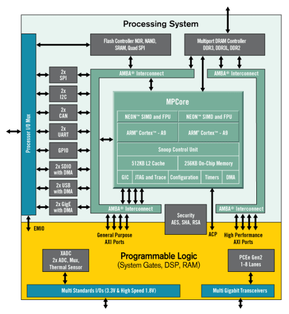
ZYNQとは?
Xilinx Zynq®-7000 All Programmable SoC (AP SoC) ファミリーは、ARM系プロセッサのソフトウェア開発とFPGAのハードウェア開発をプログラムによって可能にしている。これにより、CPU,DSP,ASSPや特定用途向けのICが統合された一つのデバイスを高速化させることが可能となる。
Vivado, SDK & Board Support Filesのインストール
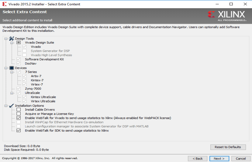
システムをデザインする前に、 Xilinx Vivado Design Suiteをインストールする必要がある。Xilinx Vivado Webpack は無料のバージョンであり、 Digilent Wikiによってチュートリアルが提供されている。
Vivadoをダウンロードする際、SDKをインストールするため、Design toolsの中にある"Software Development Kit“をクリックする必要がある。もしクリックし忘れてしまっても、再びインストーラーに戻れば"Software Development Kit“をインストールすることが可能である。
Vivadoのダウンロードとインストールが終了したら、 ボード上の異なるインターフェースや周辺機器を決定するためのZYBO boardファイルをローカルのXilinx Vivadoフォルダに入れる必要がある。これは後でIPとSDKを正常に構築するのに必要になる。Digilentはこの工程のガイドラインを以下のURLで公開している。
https://reference.digilentinc.com/reference/software/vivado/board-files?redirect=1
注意:Vivado board ファイルのインストールガイドラインでは、board_filesをローカルフォルダに移すよう指示されている。しかし、私は必要なファイルのみコピーすることをお勧めする。(つまり、vivado-boards-master\new\board_filesにあるzybo folderのみコピーする)。そうしなければ、デザイン中に無用なエラーが生じてしまうだろう。
プロジェクトの作成
それでは、このガイドライン(getting started guide )に従って、 Digilent ZYBOを使った入門プロジェクトを作ってみよう。
プロジェクトの概要
このプロジェクトでは、ボード上のLED(LD0-LD3)を4つのスイッチ(SW0-SW3)を使って操作していく。また、ボード上のボタン(BTN0-BTN3)を押すと、コンピューターのターミナルに様々なメッセージが表示されるようにする。
デザインの流れ
- Vivadoを開き、Zyboボードを選択する。
- 新しいVivadoプロジェクトを作成する。
- 新しいプロジェクト内に空のblock designを作成する。
- IP Integratorを使って必要なIPブロックを追加し、ハードウェアデザインを作成する。
- ブロックデザインを適用し、保存する。
- HDL system wrapperを作成する。
- 設計したデザインを実行する。
- Bitファイルを作成する。
- 作成したBitファイルを含んだハードウェアデザインをSDKツールに送る。
- SDKを起動する。
ハードウェアデザインの流れ
ハードウェアのデザインを作成する際は、この getting started guideのステップ2から6に従う。以下に注意点を示す。
- Run Block Automationによって、マイクロプロセッサが必要とする基本的な機能についてのinputを利用できる。
- "3.4) Double-click on new axi_gpio_0 core that was just added to bring up the customizing window. Under the IP Configuration tab check the Enable Dual Channel box. Click OK.", を行うことで、SW と BTNの 2つの入力を作成することが出来る。それぞれのaxi_gpio コアが32ビットのシングルもしくはデュアルGPIOチャンネルをサポートしている。今回のプロジェクトでは、それぞれのチャンネルに対して4ビットしか必要としない。詳細はこのAXI GPIO Guideで見つけることが出来る。
- "3.5) Add another GPIO core by repeating step 3.3 but do not enable dual channel."を行うことで、LED用の出力を一つ作成できる。
- Run Connection Automation によってand/orポートをI/Oポートに関連付けることが出来る。
- デフォルトでは、UARTインターフェースの一つ(UART1)がZYNQ IPに配置されている。リファレンス: http://blog.dev-flow.com/en/8-first-use-of-the-zynq-7000-processor-system-on-a-zynq/.

ソフトウェアデザインの概要
ソフトウェアのデザインを作成する際は、このgetting started guideのステップ7からステップ10に従う。以下に注意点を示す。
“src”フォルダの中にある"helloworld.c"(getting started guideのステップ9.4参照)を開くと、以下で示す方法で定義済み関数やライブラリの詳細を見ることが出来る。
関数/ライブラリをドラッグして反転
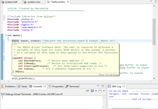
先ほど指定した範囲を右クリックしてOpen Declarationを選択

ソースコードとコメント
/*****************************************************
Getting Started Guide for Zybo

This demo displays the status of the switches on the
LEDs and prints a message to the serial communication
when a button is pressed.

Terminal Settings:
   -Baud: 115200
   -Data bits: 8
   -Parity: no
   -Stop bits: 1

1/6/14: Created by MarshallW
****************************************************/

/*include libraries from Xilinx*/
#include <stdio.h>
#include "platform.h"
#include <xgpio.h>
#include "xparameters.h"
#include "sleep.h"

int main()
{
   XGpio input, output; /*Declare two structure input & output. XGpio is*/
   int button_data = 0; /*Declare & Define initial button value*/
   int switch_data = 0; /*Declare & Define initial switch value*/

   /*Initialize the XGpio instance provided by the caller based on the given DeviceID.*/

   XGpio_Initialize(&input, XPAR_AXI_GPIO_0_DEVICE_ID);	/*We define AXI_GPIO_0 as inputs - BTN & SW*/
   XGpio_Initialize(&output, XPAR_AXI_GPIO_1_DEVICE_ID);/*We define AXI_GPIO_1 as inputs - LED*/

   XGpio_SetDataDirection(&input, 1, 0xF);			/*set first channel of input tristate buffer to input*/
   XGpio_SetDataDirection(&input, 2, 0xF);			/*set second channel of input tristate buffer to input*/

   XGpio_SetDataDirection(&output, 1, 0x0);		/*set only channel of output tristate buffer to output*/

   init_platform(); /*Initialize the platform hardware resources*/

   /*Indefinite loop - running forever*/
   while(1){
      switch_data = XGpio_DiscreteRead(&input, 2);	/*Read the switch (SW) value*/

      XGpio_DiscreteWrite(&output, 1, switch_data);	/*Write the switch (SW) value to LED (LD)*/

      button_data = XGpio_DiscreteRead(&input, 1);	/*Read the button (BTN) value*/

      /*Set up if-else-if statement to print message in the
       *UART terminal. This depends on whether one or
       * more buttons are pressed
       */

      if(button_data == 0x0){} /*If no button is pressed, do nothing*/

      /*If button value is binary 0001 (decimal 1), button 0 (BTN0) is pressed. Use pre-defined function Xil-printf
       * to print the message in the terminal
       */
      else if(button_data == 0x1)
         xil_printf("button 0 pressed\n\r");

      /*If button value is "binary 0010 (decimal 2)", button 1 (BTN1) is pressed. Use pre-defined function Xil-printf
       *to print the message in the terminal
       */

      else if(button_data == 0x2)
         xil_printf("button 1 pressed\n\r");

      /*If button value is "binary 0100 (decimal 4)", button 2 (BTN2) is pressed. Use pre-defined function Xil-printf
       *to print the message in the terminal
       */

      else if(button_data == 0x4)
         xil_printf("button 2 pressed\n\r");

      /*If button value is "binary 1000 (decimal 8)", button 3 (BTN3) is pressed. Use pre-defined function Xil-printf
       *to print the message in the terminal
       */

      else if(button_data == 0x8)
         xil_printf("button 3 pressed\n\r");

      else
         xil_printf("multiple buttons pressed\n\r"); /*All other values, print "multiple buttons pressed*/

      usleep(200000);			/*Delay 200000us*/

   }
   cleanup_platform(); /*Clean up all caches*/
   return 0;

}
プロジェクトの実行
プロジェクトを実行する方法はステップ11で説明されている。FPGAのプログラミングが終了し、アプリケーションが正常に完成すると、以下の結果が得られるだろう。
- 4つのスイッチ(SW0-SW3)を押してみよう。対応するLEDが光るはずだ。
- ボタン(BTN0-BTN3)を押すと、シリアルポート上に“button x pressed”というメッセージが流れるだろう。
