Electronics designs that are out of this world (literally!)
Follow article
 Dave from DesignSpark
How do you feel about this article? Help us to provide better content for you.
Dave from DesignSpark
Thank you! Your feedback has been received.
Dave from DesignSpark
There was a problem submitting your feedback, please try again later.
Dave from DesignSpark
What do you think of this article?
We love hearing a little more from our community members, we recently met James Nadir when he contacted us for help regards a PCB he was designing, which, excitingly enough, is destined for the International Space Station! We wanted to know more about what James does, so James, in his own words, tells us a little bit more about the various projects and designs, he, his students and associates are involved with whilst working as a mentor at the Valley Christian High School.
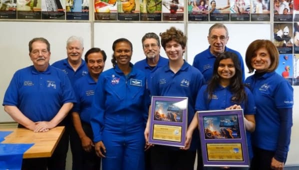
James Nadir (2nd left) with some of his associates at VCHS
'Hello, my name is James Nadir and I am a mentor at Valley Christian High School (VCHS), we help students across the US and around the world to put their experiments aboard the International Space Station (ISS) for low cost and within 9 months. In-flight data and photos are returned to students about every 2 weeks once their experiment is activated aboard the ISS. VCHS provides the entire ecosystem (hardware, software, logistics, module delivery/retrieval, and training) to our partner schools and is open to any school or university. This ecosystem enables students to develop their experiments much as they would a Raspberry Pi or Arduino project without having to become experts in communication protocols, NASA system operations, flight specialists (i.e. without being “rocket scientists”... ahem...). While the emphasis is on the science and engineering of an autonomous experiment aboard the ISS, the knowledge and training are useful for any science and engineering discipline that students pursue in their future careers. For more information, there is a recent article published in Nature’s Publication Journal (NPJ Microgravity) called “Low-Cost Hitchhikers guide to the ISS” which describes the collaterals and methods used in the space program.
Prior to volunteering at VCHS my previous life was at Intel Corporation where I worked on the x86, Pentium and Itanium product families as a principle engineer. I also developed the first synthesis libraries (used to translate a logical description into physical designs), developed post-processing software to improve synthesised (auto placed and routed) implementations performance, and led circuit design teams to develop the first and second level caches.
A solution for the sophisticated designs
Our program started with the simplest software possible to make it possible for any student to develop software, learn about electronics, and implement their payload PCBs which interface to the on-board processors. This was fine in the beginning but by the second or third-year student experiments have become much more sophisticated as students became involved and mentored by university professors and other scientists who wanted to do a microgravity experiment but couldn’t easily do so on their own. We needed to move to the next generation of tools to support much more sophisticated experiments than we originally anticipated. We looked at Sunstone, Eagle, CircuitMaker before selecting DesignSpark.
DesignSpark was very intuitive, has a low learning curve to start useful work and has high-end features such as auto place and route. DesignSpark was ideal because it enabled a connection to be established between circuits and mechanical engineering by its ability to export a 3D image. This is very exciting because circuit design and mechanical design are no longer decoupled “problem over the wall” interactions. The electrical engineering student produces a 3D image which is then imported into a 3D CAD tool (such as DesignSpark Mechanical, or AutoDesk’s Inventor) for interference analysis. The effort to develop a custom component (even a non-electrical component such as a fluid bag or observation chamber) and include it as part of the PCB’s 3D image is very low but very valuable for mechanical interference analysis.
In addition, many students want to develop skills that are valued in the industry. For example, learning BASIC (even though it is still used) isn’t as exciting as learning the language “du jour” such as Java, C#, C++ or Python. It is the same with a PCB tool, DesignSpark is very appealing but without the steep learning curve.
Modern interfacing
We are now developing our 3rd generation ecosystem of which DesignSpark PCB and DesignSpark Mechanical are being integrated. We are of course stumbling as we try to do things with the tools that were not originally anticipated by the developers. But we have workarounds for all of the issues to date and have excellent support from the DesignSpark help desk. Our first attempt at using DesignSpark PCB was surprisingly easy and yielded a usable design that we are now fabricating at OSH Park. The design used manually placed components (left in the picture below), auto-routed, and then manually modified afterwards (right).
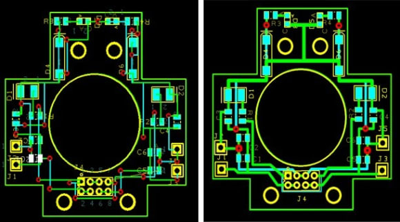
This was a particularly difficult test due to the centre-hole obstacle in the board. The auto-routed successfully navigated around this obstacle without special “keep out” attributes. We could have stayed with auto-routed version but wanted to see how easy it was to do manual edits (it was easy but took about 1 hour).
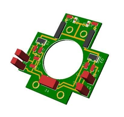
We then produced a 3D model of the board which we pulled into AutoDesk’s Inventor for interference analysis. This was much easier than we anticipated. DesignSpark PCB uses the outline on the silkscreen layer to establish a component footprint and its height is easily defined in the component’s property “height” attribute. This is the 3D image that we used to check for mechanical interference.
We are now evaluating DesignSpark Mechanical as an alternative 3D CAD tool for students who haven’t taken the “Principles of Engineering” class (which uses Inventor CAD) but have a need to produce a 3D printed part for their ISS experiment.
Both DesignSpark PCB and DesignSpark Mechanical use modern interfaces compatible with touchscreen displays. The intuitiveness of their interfaces makes it very appealing for students and mentors.
Transmitting the data
Below is an image of an unhoused experiment module showing the finished PCB design. The PCB is used to control two peristaltic pumps and to provide photo illumination for the camera which is peaking through the hole in the middle of the PCB. Behind the pump assembly is the microprocessor board containing digital and analog IO, Photo buffer RAM, camera support, sensors and the watchdog slave processor. Behind that is the development system with the master processor and watchdog. The master processor is the same board used in the flight system and contains all the functions necessary to retrieve and transmit student data during flight to ground. In front of the pump assembly is the rapid prototype board which students use to quickly discover issues with their flight software and hardware. It can be populated with through-hole components and used to directly drive an external breadboard.
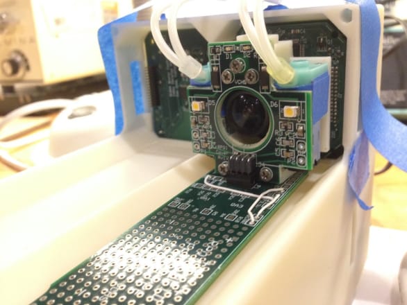
The finished PCB with peristaltic pump behind
50% cheaper and impressive!
Our initial “free” PCB tools are the front end to PCB fabs. With DesignSpark PCB, we are now decoupled from the fab and are able to reduce our costs significantly (over 50%). The ease of use and fast learning is an additional cost saving which we haven’t quantified, but we know is real.
Overall, I am very impressed with the software’s low learning curve and intuitive interface. The ability to export 3D images creates a link between electrical and mechanical design that has alluded us in the past (mostly due to the high overhead of custom components) is now easily obtainable. The ability to import complex board shapes from a 3D cad tool (XDF format) is also a bonus for some of our convoluted PCB shapes needed to fit within the small enclosure of the experiment housing.
Feature requests
- We import complex board shapes using the SDF as a silkscreen layer and then matching its shape using the PCB outline tool. Afterwards, we can import the design into a template that can be accessed through the Translate to PCB wizard. It would be much more convenient if we could import the XDF directly to the board layer.
- Another nice feature is the ability to have predefined “PCB templates” for our students with pre-placed connectors and other mechanical parts which are required for all our payload PCB boards. It is desirable if these templates were pre-routed or were defined in such a way that “unroute all nets” would not undo the template’s routeing.
- Producing Gerber files is painful and error prone for students. We used to use Robot Room’s “Copper Connection” to generate the Gerbers and drill files automatically with no manual renaming or special drill configuration steps. Unfortunately, Copper Connection was purchased by ExpressPCB (to improve their layout tools and stencil generation). Lucky for me, I already have a purchased executable so I can still generate low cost stencils but it is now off the market for others. It would be good if DesignSpark could generate Gerber files for different vendors such as OSH Park.
- We are having some issues with the tool generating the inner power planes but this could be operator error. If it is a bug, I would recommend it to be a high priority fix.
The VCHS International Space Station Program
VCHS ISS program is an outreach program to all students of all faiths and beliefs. It has successfully pulled “at risk” students out of gangs and away from drugs and put them on a rewarding path to engineering and sciences. It integrates the more privileged with the less privileged students. And one of the most important benefits is that students learn to operate as teams where no one person is more important than the other (i.e. a leader is just a person with a different task to arrange and coordinate activities and if one student fails then the whole project fails). This is unlike the classroom environment where students compete against each other and all do the same thing under the guidance of a teacher. In the ISS program, the student learns that there is no one right answer, to be innovative and resourceful, and is prepared to enter industry environment. I heartily encourage all schools and colleges to become involved in this student outreach program and to contact VCHS for the details.'
We are DesignSpark would like to thank James for taking the time to tell us all about the projects he and his students are involved with that are destined for the International Space Station, thank you James! From our perspective, here at DesignSpark, it’s really good for us to know that DesignSpark DNA is orbiting the Earth as we speak!