DSPCB - Using Pad Style Exceptions for reduced inner layer copper pad size
Follow article
 Dave from DesignSpark
How do you feel about this article? Help us to provide better content for you.
Dave from DesignSpark
Thank you! Your feedback has been received.
Dave from DesignSpark
There was a problem submitting your feedback, please try again later.
Dave from DesignSpark
What do you think of this article?
Note: to use the below features, you will need DesignSpark PCB with an Engineer subscription.
Here we illustrate the application of the Pad Style Exceptions to allow any through-hole pad to have a reduced pad size on the inner layers. This allows a greater inter-pad area for routing.
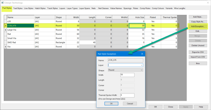
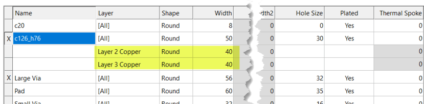
Here we are using a Pin Grid Array socket as an example, add your component into your design and in the PCB editor launch the Design Technology. Now select the pad used for the component and click the <Add Exception> button and a new window will open for you to customise the pad for a selected layer.
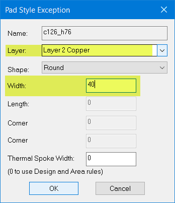
Here we enter a smaller pad diameter of 40 thou on Layer 2 Copper.
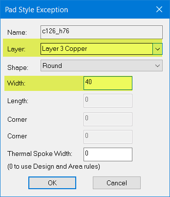
Repeat for other layers as required.
All the settings are now complete.
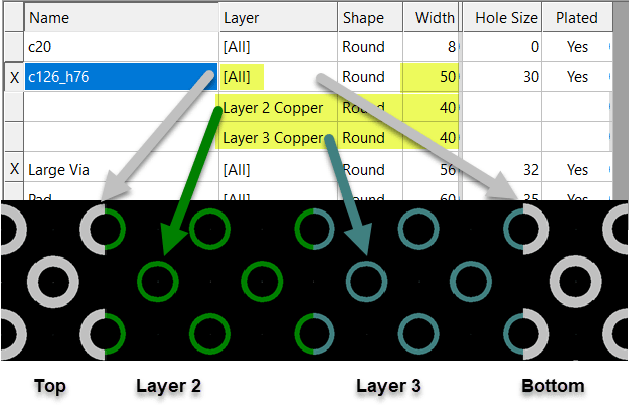
You will see that the two pad style exceptions are now listed under the pad.
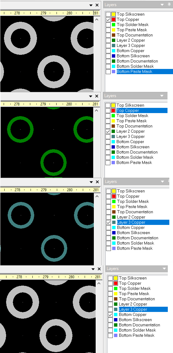
Click <Apply> and the PCB design is updated.
Viewing the layers individually shows the different pad sizes by layer as were defined.
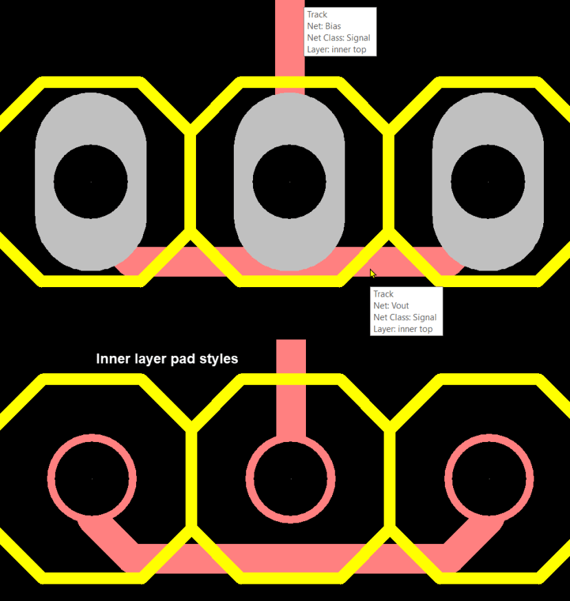
This Pad Style Exception can be of benefit for any pad such as where you require a large pad for soldering but a smaller pad on another layer as shown below.
This 0.1" pin header has oval pads by default on all layers.
Adding pad style exceptions for the inner layers allows tracks to be routed much closer to the pad without reducing the soldering pad area on the outer layers.
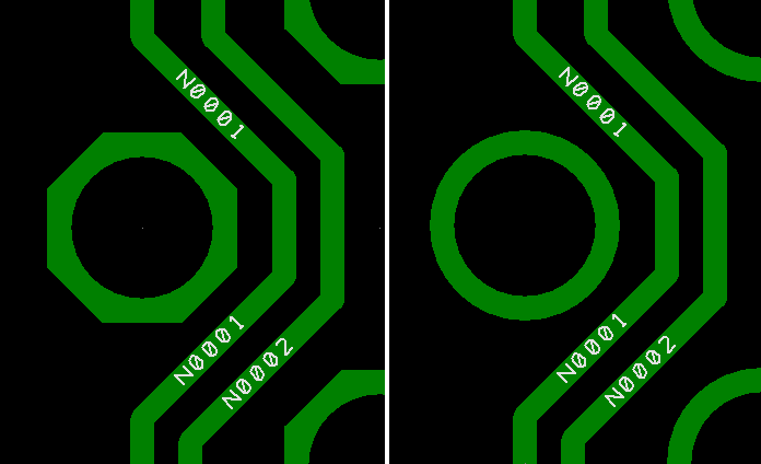
The new Pad Shapes Hexagon and Octagon in v10 can also be used to your advantage when routing in a limited space by allowing the pad area to be slightly larger than a round pad.
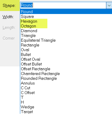
Below shows the increased pad area with the Octagon pad compared to the Round pad.
Other related articles: