DSPCB - Creating "solder jumpers"
Follow article
 Dave from DesignSpark
How do you feel about this article? Help us to provide better content for you.
Dave from DesignSpark
Thank you! Your feedback has been received.
Dave from DesignSpark
There was a problem submitting your feedback, please try again later.
Dave from DesignSpark
What do you think of this article?
Pads can be used to provide a 'jumper' function by applying a solder bridge. These can be more compact than using a pin header with configurable jumper links. Although still user-configurable they should be used only for jumpers that the user is unlikely to need to change.
Some examples are chip address pins, 50Hz/60Hz configuration and also debugging aids for field servicing and development where you may require to isolate grounds at a common point (star point) and separate analogue, digital and power ground connections.
Many modern PCBs that provide solder jumper options often simply use standard surface mount pads. There is nothing inherently wrong with this approach, but it has been known to cause confusion and be considered a missing component!
Also, solder tends to naturally form a ball when melted so the traditional split circular pad is still considered desirable.
For solder jumpers consisting of two semi-circular copper pads closely spaced, we now illustrate how to create these.
1. From the Library Manager select the PCB Symbol Tab, select the destination library and click <New Item>.
Note you can also select the required Technology File to use for the footprint from the <Tech Files…> button or the ‘last used’ will be used.

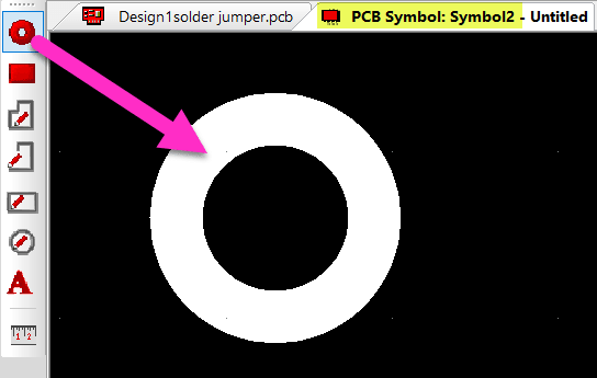
2. In the PCB Symbol Editor, add a Pad, right click and select Style.
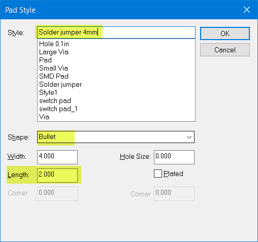
3. Provide a name for the new style.
Select “Bullet” and enter the Width and Length you require, the Length must be a minimum of half the width (which will produce a semicircle).
Set the Hole Size to Zero and uncheck “Plated”.
Click OK to save.
4. You now have the pad as you defined.

5. Add a second pad and rotate and position for the required gap.

6. If you require that there is no solder mask between the pads, add a shape on the Top Solder Mask layer.
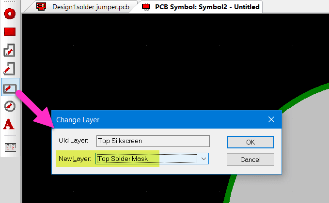
7. Select the added shape and in the Properties check the “Filled” check box.

8. The footprint is essentially now complete, we just have to change the layers to restrict it to the top layers.

9. Select a pad and use the shortcut “L” to change the layer. Repeat for the second pad.

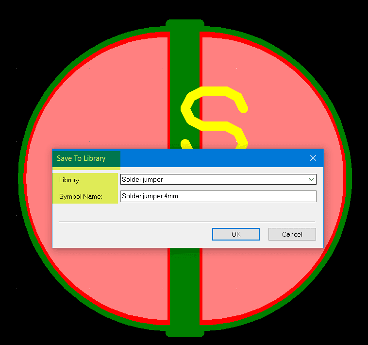
10. Now use the “Save” icon and save to your required library with the desired symbol name.
11. In the Library Manager – PCB Symbols tab, you can preview your footprint.

12. Now create a component.
Create a schematic symbol or use an existing symbol.
From the Library Manager – Components Tab, select <New>.
Select the Schematic Symbol and the PCB symbol and complete the text fields. Click <OK>.

13. In the Editor, complete the Pin Mapping and then click the "Save" Icon to finalise the component which is now ready for use in all your designs.

Use the component as normal.
Using "Add Component" shows the component preview.

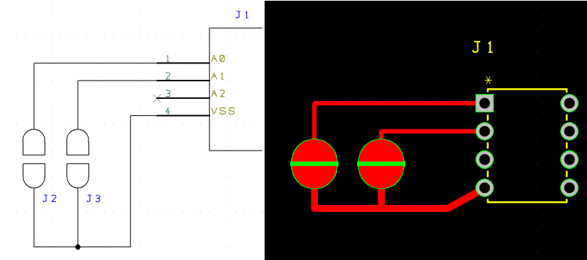
Here we show our example solder jumper in a schematic and translated to a PCB design.
The component was designed for the top copper layer, simply use the Flip command to place it on the bottom copper layer.
With an Engineer subscription, DSPCB users can also control the paste mask opening using pad-style exceptions using the techniques described here: