DesignSpark PCB - Slotted Pads
Follow article
 Dave from DesignSpark
How do you feel about this article? Help us to provide better content for you.
Dave from DesignSpark
Thank you! Your feedback has been received.
Dave from DesignSpark
There was a problem submitting your feedback, please try again later.
Dave from DesignSpark
What do you think of this article?
DesignSpark PCB makes it very easy to add slotted pads to your component footprint.
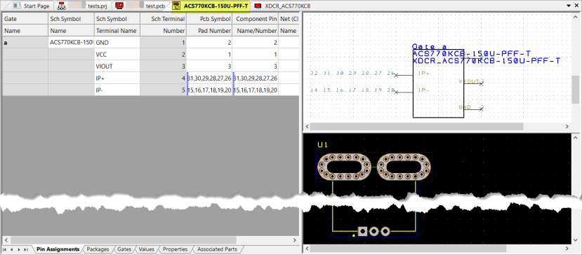
Here we examine the Allegro ACS770 current sensor https://uk.rs-online.com/web/p/current-sensor-ics/1709142
The footprint provided in the datasheet is:
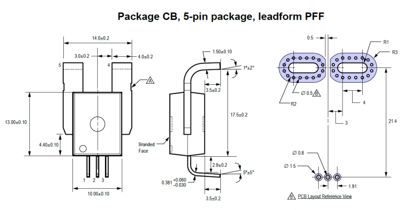
The high current pads also have a non-symmetrical shape plus vias.
To illustrate the simplicity of creating a slotted pad we use a SnapEDA component model which has symmetrical pads but does not have a slot. As a note online component libraries from any source will often not include slots in a pad, the reason is that most ECAD software handles slots in a different manner and it is for you to customise as required.
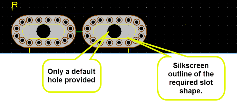
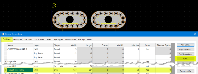
Examining the pad details in the Design Technology - Pads tab we can see it is defined as an oval pad 354 thou x177 thou with a 79 thou hole.
Select this pad and then click <Edit>
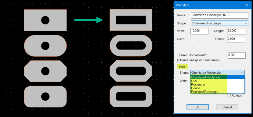
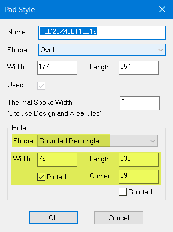
You are now presented with the Pad Style window and can choose a shape for the hole!
Here we simply select the Rounded Rectangle for the hole and enter the required dimensions.
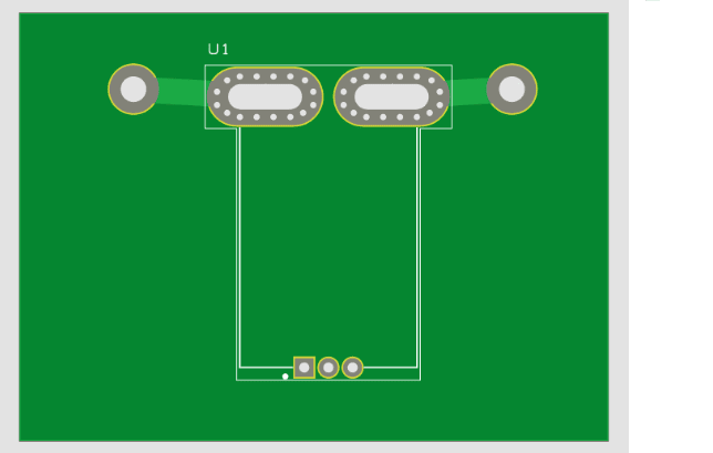
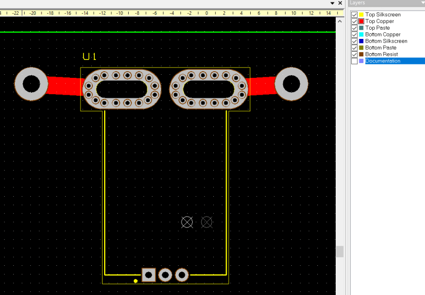
With the slots now in the pad, the updated pad can be saved and the component in the library will be updated as below.
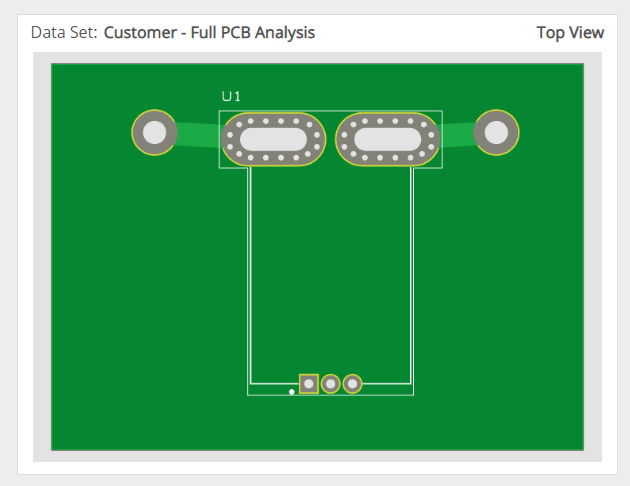
It is now ready for use in your design as shown in this simple example.
The Gerber plot files were produced for this simple PCB and checked in the Ucamco Online Reference Gerber Viewer.
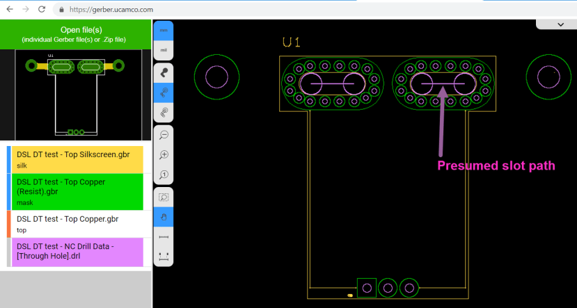
Also, the validity of the Gerber and drill files were successfully confirmed with the EuroCircuits PCB Visualiser.
The pad style/shape is selected as normal, if you then set a hole size this will be the default used as the slot width when generating a slot.
The Hole shape can be selected from the pull-down options and here we show them matching the pad shape.