Create a custom PCB Board: Part 3 - Component Positions
Follow tutorial
 Dave from DesignSpark
How do you feel about this tutorial? Help us to provide better content for you.
Dave from DesignSpark
Thank you! Your feedback has been received.
Dave from DesignSpark
There was a problem submitting your feedback, please try again later.
Dave from DesignSpark
What do you think of this tutorial?
This tutorial requires:
DesignSpark PCB V11.0.0The PCB we have completed so far in parts 1 and 2 is useful as it as it stands and may be all that you require for your own custom board example. For this Arduino example we will also add connector positions as these are in fixed locations.
But, why not just add the connector components?
It is tempting to add these to the PCB design now, however "location markers" for the connector positions allows the PCB to be added to any project and follows the design methodology of DesignSpark PCB where the design is created in the schematic and forwarded to the PCB. This avoids any issues from the back annotation function (PCB to the schematic) which does not support added "components".
Adding the location markers
For this example we illustrate how to add "location markers" on the PCB. These will be simple symbols on the documentation layer.
For the connectors we will identify the pin 1 location first with a square pad on the documentation layer. Select "Add pad" as normal but before placing, press "L" to change the layer to "Documentation". Ignore the warnings.
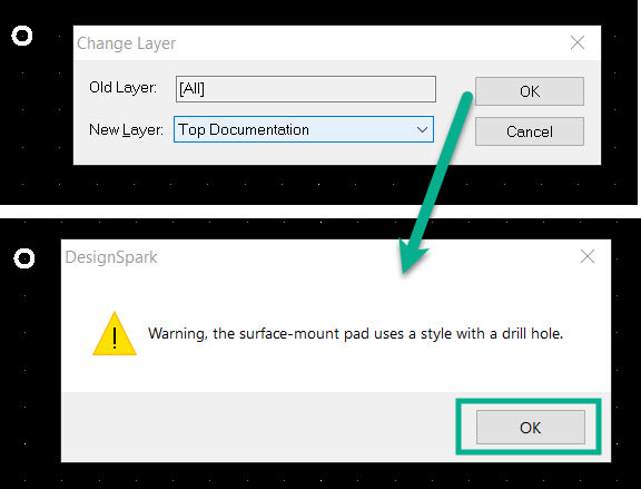
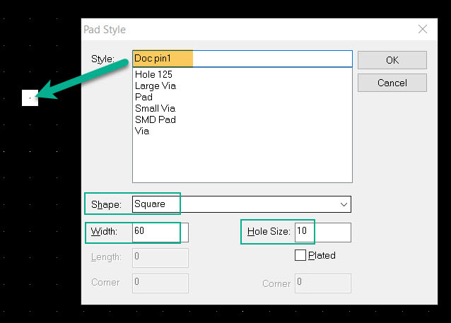
With the pad still highlighted we can change the properties and add it to our design. Press the short cut key "S" to change the Style. Here we have named it Doc pin1 to represent "pin 1 on the documentation layer". Typical values are shown, uncheck the "plated" check box.
With the pad still highlighted press the short cut key "=" and enter the relative coordinates to place it. The pad can be confirmed to be on the correct layer using the tool tip.
The correct layer can be confirmed with the tool tip.

Place all the pin1 reference pads.
Now we can add the general pins by the same method.

This can be placed with the "=" key as before and can be at the maximum pin number for each connector only (or in as many places as required to allow the connector to be placed accurately at the location) as we do not require every position as it is purely for location of the component.

To avoid confusion with adjacent connectors draw an outline around the pads to identify the connector. Use the "Add Closed Shape" tool.
Note: Setting a snap to grid of 1/4 will help in generating the shape as it does not require to be an accurate representation.

Note: If the close shape appears "filled", select the shape, right click and click "properties, then uncheck the "filled" option.

Now repeat for all other connectors.

We now require to add some identification of which connector is which. This needs to be a descriptive text as we do not know at this step what the final component reference will be assigned as this depends on how you create the schematic.

Now complete the layout with any additional features required, such as the ICSP connector and also the location of the Power and USB connectors as you may wish to avoid these areas with certain components in your design.
Adding the ICSP connector
This is a good example of how to use the "Relative Origin". The supplied drawing provides (See Part 1) shows this at an unusual location (Check other documents for accuracy), but these will be used in this example, Pin 1 is located at 2505.512, 1198.031.
Place the pin 1 reference pad at the above location using the "=" shortcut. Then set the relative origin at this item. The normal pad locations can then be positioned relative to this at the 100mil offsets. Note if you examine the image carefully, you can see the relative origin marker central to the square pad.

The Power and USB connector locations are now added and the PCB is complete ready to use.
