What is FET: A Guide on FET
Follow article
 Dave from DesignSpark
How do you feel about this article? Help us to provide better content for you.
Dave from DesignSpark
Thank you! Your feedback has been received.
Dave from DesignSpark
There was a problem submitting your feedback, please try again later.
Dave from DesignSpark
What do you think of this article?
I’ll walk you through the FET (Field Effect Transistor) in detail and cover each and everything related to FET including FET definition, symbol, working, characteristics, types, and applications.
Let’s get started.
Definition:
The FET(Field Effect Transistor) is a three-terminal electronic device used to control the flow of current by the voltage applied to its gate terminal. The three terminals in this device are named drain, source, and gate.
- Source: It is a terminal through which charge carriers enter the channel.
- Drain: It is a terminal through which charge carriers leave the channel.
- Gate: This terminal controls the conductivity between source and drain terminals.
FETs are also known as unipolar transistors as opposed to BJTs that are bipolar transistors. In FETs, either holes or electrons are used for the conduction process. But conduction process doesn’t involve both charge carriers at the same time. FET transistors usually come with high input impedance at low frequencies and display instant operation, high operation, are robust and cheap, and are used in many electrical circuits. The low power consumption and low power dissipation make this device an ideal fit for integrated circuits.
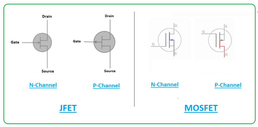
Symbol:
The following figure shows the symbol of MOSFET and JFET transistors that are the two main types of FET transistors.
Working:
The FET is an electronic device that contains charge carriers, either electrons or holes that flow from source to drain terminals through the active channel. The conductivity process is controlled by applying the input voltage at the gate terminal.
The current-carrying path that exists between the source and drain terminals is known as “channel” which can be composed of either N-type or P-type semiconductor material.
The working of N-Channel JFET can be described as follows by taking two different cases:
Case 1:
In case 1, the voltage at the gate pin is zero, and voltage Vds is applied between drain and source terminal as shown in the figure below.
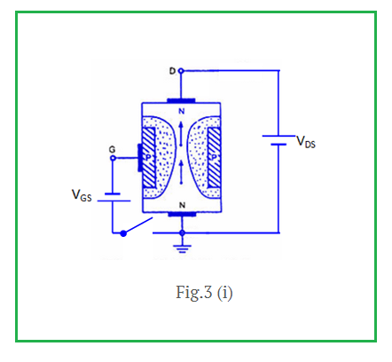
In this case, the two pn-junction across the bar sides generates a depletion region. As a result, electrons flow from source to drain terminal through a channel that stands between the depletion layers. The channel width and current conduction through the bar are determined by the size of the depletion layers.
Case 2:
The depletion layer width increases when the reverse voltage is applied across Vgs gate and source terminals. This results in reducing the conduction channel width and would increase n-type bar resistance.
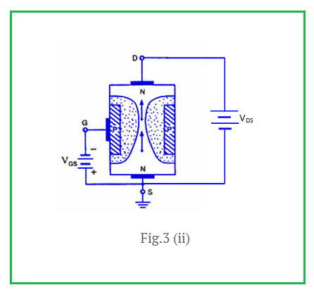
Hence, the current from source to drain terminals reduces. However, when the reverse-biased voltage on the gate terminal is decreased, it would also decrease the depletion layer width, and as a result, the conducting channel width would increase.
This is the working of N-Channel JFET that works similar to P-Channel JFET. The only difference is the charge carriers. In the case of N-Channel JFET, charge carriers are electrons, while they are holes in the case of P-Channel JFET.
Characteristics:
The following figure shows the characteristics curves of JFETs:
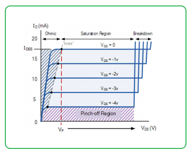
A: Ohmic Region:
In the ohmic region when Vgs = 0 the JFET will behave as a voltage-controlled resistor and carries a very small depletion layer of the channel.
B: Cut-Off Region:
The Cut-Off region is also called a Pinch-off region where the gate voltage Vgs is enough to force the JFET to behave as an open circuit since the resistance of the channel is maximum.
C: Saturation Region:
The saturation region is also called the active region where conduction of the device is very high that is controlled by the applied voltage on the Vgs gate and source terminals. In this condition, drain-source Vds voltage will have little or no effect.
D: Break Down Region:
In this region, the voltage across the source and drain terminals Vds is very high that breaks down the JFET resistive channel and allows the flow of uncontrolled maximum current.
The drain current Id increases linearly with the voltage on source and drain terminals Vds. As the Id increases, the ohmic voltage drop across the channel region and source terminal will reverse bias the junction and as a result, the conduction of the channel remains constant. The Vds voltage at this position is known as “pinch-off” voltage.
Types:
The FET transistors are divided into two main types:
1: JFET
2: MOSFET
1: JFET
JFET (Junction Field Effect Transistor) is a three-terminal electronic device and is a type of FET transistor mainly employed to develop amplifiers and are used as electrically controlled switches. JFETs are voltage-controlled devices as they don’t require biasing current to start the transistor action.
A JFET exists in an ON state when no voltage is applied between the source and gate terminals. However, when voltage is applied at source and gate terminals, this device will show resistance in the flow of current and allows only limited current flow between the source and drain terminals.
The JFETs are further divided into two types:
- N-Channel JFET where conduction is carried out by the movement of electrons.
- P-Channel JFET where conduction is carried out by the movement of holes.
The N-Channel JEFTs are preferred over P-Channel JFET in many electronic applications because the mobility of electrons is better than the mobility of holes.
2: MOSFET
The MOSFET (Metal Oxide Semiconductor Field Effect Transistor) is a semiconductor device mainly used for amplification and switching applications in electronic devices.
MOSFET is a voltage-controlled device as the input voltage on the gate terminal controls the conductivity between the source and drain terminal.
MOSFETs are further categorized into two main types:
- N-Channel MOSFET where conduction is carried out by the movement of electrons. This transistor is highly efficient and comes with low resistance and occupies a lesser area.
- P-Channel MOSFET where conduction is carried out by the movement of holes. This transistor is less efficient and carries high resistance and occupies a large area.
Applications:
The FET transistors are used in the following applications.
- Analog Switch
- Current Limiter
- Cascode Amplifier
- Chopper
- Phase Shift Oscillators
- Multiplexer
- Buffer Amplifier
Hope you’ve found this article useful. If you have any questions, you can approach me in the section below. I’d love to assist you the best way I can. Thank you for reading the article.