Dealing with Conducted Noise in Electronic Circuits
Follow article
 Dave from DesignSpark
How do you feel about this article? Help us to provide better content for you.
Dave from DesignSpark
Thank you! Your feedback has been received.
Dave from DesignSpark
There was a problem submitting your feedback, please try again later.
Dave from DesignSpark
What do you think of this article?
Frustrating Faults
Many students studying electronic engineering will have had one or other of these experiences while developing project hardware:
- The plug-in breadboard prototype works perfectly despite the fragile mess of interconnecting wires. But after ‘tidying up’, bundling all the wires together in neat looms just before presenting the project to examiners, it becomes unreliable or stops working altogether.
- As above, but this time a nice PCB or soldered stripboard has been created with the same embarrassing result.
Sounds familiar? The most frustrating part of it, is that the ‘upsets’ are usually intermittent making the cause hard to trace. It seems counter-intuitive that a bench lash-up with wires all over the place should work, but a neat PCB doesn’t. Of course, breadboards are not immune from faults, but they’re most likely to be constant. For instance, wires plugged into the wrong hole or displaced while relocating the project. So why do weird things start happening when the wiring is tidied up? All electronic components generate electrical noise, degrading the signals being processed. Component quality is thus important, but poor interconnection design can mean the difference between good performance and non-functionality. This is because we are talking about ‘noise’ induced into a conductor (wire or PCB track), from an adjacent conductor by capacitive, inductive or common-impedance coupling. It’s described as noise because it’s an unwanted signal, but it’s not like the Added White Gaussian Noise (AWGN) or thermal noise generated by all electronic components. This noise originates from a valid signal carried by that adjacent conductor. Another name for it is Crosstalk.
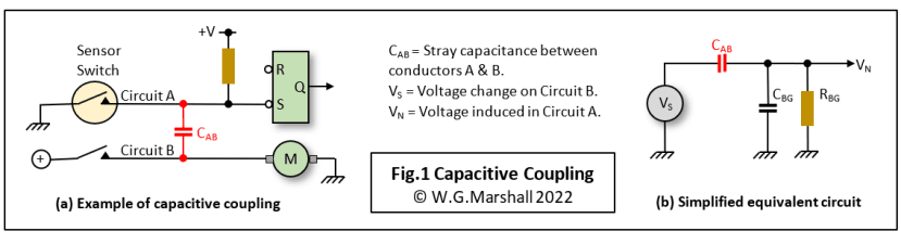
Capacitive coupling
It’s easy to understand the concept of capacitance between two adjacent parallel wires or PCB tracks (Fig.1). In this example, trouble occurs when the motor is turned off while the sensor switch is open. The sudden fall in the motor voltage to zero drags down the Set input due to the stray capacitance CAB linking the two circuits. Despite the sensor switch being open, the flip-flop output Q is thus set to a logic 1. Obviously, the main cause of this unwanted crosstalk is the running of signal wires close together in a nice neat loom! That’s why a messy breadboard with no signal wires running parallel with each other is so much less prone to upsets. There are two other factors though:
- Circuit B operates with a higher voltage than Circuit A.
- Circuit A will have a sensitive high-impedance input.
Inductive coupling
A similar setup to the above example is also prone to inductively-coupled noise (Fig.2). Once again, it’s those loomed wires or long parallel PCB tracks that are the main cause of trouble. It may seem strange, but even straight wires possess a small amount of inductance. And what do you get when you place two inductors side-by-side? You make a transformer with mutual inductance M. For maximum effect:
- Circuit B will be operating with very high currents; amps rather than milliamps.
- Circuit B will be switching those currents at fairly high frequencies.
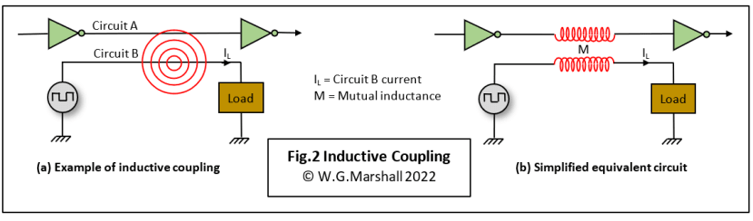
Current spikes will be induced in digital Circuit A generating false clock edges every time Circuit B switches.
Common-impedance coupling
It frequently comes as a shock (not always literally) to an electrical engineering student that wires are not perfect conductors with zero impedance. Or that notional insulators do conduct under certain circumstances. The two types of interference discussed so far, require circuit conductors to run closely in parallel for a distance. How great a distance depends on the current, voltage and most importantly, the signal frequencies involved. Common-impedance coupling occurs where two circuits share the same conductor. The most common example involves the connection of circuits to the 0 volt power supply rail (Fig.3). In this case, a heavy-current circuit shares its link to 0v with that of a sensitive high-impedance input digital latch. Described like that, it seems an obvious situation to avoid. But it’s easily done when attempting to minimise the number of PCB tracks or wires needed for a prototype. The wire or PCB track in red is the critical bit and point A is where the two circuits are physically connected together.
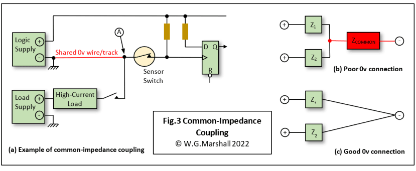
Capacitive and inductive coupling are essentially transient phenomena associated with fast-changing signals. Common-impedance brings in resistance as a factor, so there are both transient and steady-state consequences. Diagram (a) shows a normally-closed sensor switch holding the clock input of a D-type latch in a logic 0 state. The two resistors are ‘pull-ups’ which ensure that the two high-impedance inputs are held at logic 1 when no other input is present, making them less vulnerable to noise pickup. In normal operation, the sensor switch opens and the rising edge of the signal clocks the logic 1 of the D input through to the Q output. The output stays in that condition until the R input is pulsed low. Now consider what happens when the sensor switch is closed and the high-current load switched on. The effect of heavy current applied suddenly to the stray inductance of the common 0v section will cause a voltage ‘spike’ to appear at point A which could be high enough to clock the latch. Once the spike has passed, wire resistance may lead to point A sitting somewhat above zero volts reducing the logic threshold for noise clocks from elsewhere.
Diagram (b) is a simplified impedance diagram illustrating the problem. Diagram (c) on the other hand, provides the solution – don’t share 0v rails! Of course, they have to be connected together somewhere, usually back at the power supply.
Conclusion
The first thing to say is: don’t get too worried about perfect component layout and ideal interconnection when designing your project. When working with low voltages, low currents, and frequencies less than a few megahertz, just about anything will work – even with neatly loomed wiring. Here are some general guidelines for low-frequency applications:
- If the design features high-current devices such as motors, keep their power lines separate from analogue and digital power rails. The 0v or Ground lines should only meet at the power supply.
- Decouple the power supply pins of each IC to 0v with 0.1μF ceramic capacitors as close as possible to the chip. Place a 470μF electrolytic or tantalum ‘reservoir’ capacitor on each power rail where it comes onto the board. These help to block switching transients from propagating along the power rails between chips.
- Make sure the tracks or wires are large enough to handle heavy currents where appropriate. The aim is to keep the impedance as low as possible to avoid volt-drops, not just overheating.
- Never leave unused inputs on digital ICs ‘floating’. Always pull them up to the supply voltage or down to 0v with say a 10kΩ High-impedance floating inputs form an easy ‘gateway’ for noise.
There’s a lot more to the subject of electrical interference and its remedies that can be covered in a single article. There are techniques for keeping conducted noise out involving the use of ground-planes in PCBs, filtering, differential signalling, shielding and cable-twisting. There is also the problem of radiated noise from high-power RF sources, requiring shielding around whole enclosures. I hope to discuss these and other related topics in future articles.
If you're stuck for something to do, follow my posts on Twitter. I link to interesting articles on new electronics and related technologies, retweeting posts I spot about robots, space exploration and other issues. To see my back catalogue of recent DesignSpark blog posts type “billsblog” into the Search box above.