Catching a Bus: Basic Serial Communication Part 4, I2C
Follow article
 Dave from DesignSpark
How do you feel about this article? Help us to provide better content for you.
Dave from DesignSpark
Thank you! Your feedback has been received.
Dave from DesignSpark
There was a problem submitting your feedback, please try again later.
Dave from DesignSpark
What do you think of this article?
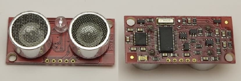
An SRF08 ultrasonic rangefinder with an I2C communication interface. The on-board MCU handles all the signal processing and data formatting, taking a great deal of the computational overhead from the host.
Most modern peripheral device chips, such as sensors and motor drivers, communicate with a controller via a serial data bus. Microcontrollers usually support one or more of three basic types: UART, SPI and I2C. How do they work and which to choose? In Part 1 we looked at one of the earliest ‘digital’ asynchronous technologies initially developed for telegraphic communication; later adapted for linking teletypewriters to computers via a UART circuit. Part 2 covered the Serial Peripheral Interface or SPI bus designed as a faster, more versatile bus to replace the old UART-based type.
Why did we need a new serial bus standard?
Philips Semiconductor (now NXP) introduced the I2C bus back in 1982, just as engineers began to develop embedded applications based on microprocessors. Back then, single-board computers (SBC) were becoming widely available, but they were physically large to accommodate the many other chips needed to support the microprocessor. These support chips, EPROM/SRAM memory, peripheral port controllers, timers, etc, invariably communicated via parallel (usually 8-bit) data busses. This meant big DIP packages with lots of pins, and of course a lot of PCB area covered in copper tracks. A typical ‘embedded’ design might have ended up looking something like Fig.1. Note that the microprocessor (MPU) lacks the Input/Output ports (GPIO) of a microcontroller (MCU); it has neither on-board peripherals nor even any program/data memory. All program instructions and data move between the MCU and the memory/peripheral chips along a bi-directional parallel data bus. Even more device pins and PCB tracks are required for the address bus and read/write control signals.
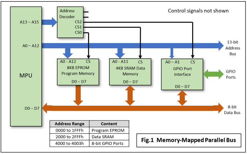
This type of parallel bus system is still in widespread use today, linking DDR SDRAM memory modules to fast 64-bit MPUs on PC motherboards. But it’s too clumsy when the priority for an embedded system is small-size and low-power rather than outright speed.
Inter-Integrated Circuit (IIC, I2C or I2C) bus
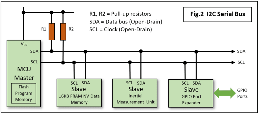
A feature of most MCUs is that non-volatile program memory, scratchpad RAM, analogue and digital port interfaces are all on-chip. A simple project may be realised with little more hardware than the MCU chip itself! However, as MCUs have become ever more complex over time, so have peripheral devices. For example, an Inertial Measurement Unit (IMU), the heart of an inertial navigation system used to be based on incredibly expensive (and heavy) electromechanical components. Then MEMS technology gave us chip-sized solid-state accelerometers and gyroscopes. Now, single-chip 9-DOF IMUs are available containing 3-axis accelerometers, gyroscopes and magnetometers. These devices often have their own on-chip MCU providing sensor fusion and serial communication with a host system. On-chip processing of sensor data relieves the host or ‘Master’ MCU of much work and may well reduce considerably both the quantity of data and the transmission rate of the serial channel. Certainly, the need for parallel bus working should be eliminated in most applications. Fig.2 shows how a huge quantity of wires or PCB tracks has been reduced to just two plus a couple of resistors. The two resistors are key to I2C operation. Unlike a UART or SPI interface, which features a pair of MOSFET transistors arranged in push-pull to drive the bus both ‘high’ and ‘low’ (but not at the same time obviously), the I2C lines can only be driven low and rely on a passive ‘pull-up’ resistor to take them high. A big advantage of this Open-Drain working is that many outputs may be wired together and no damage will result if more than one is switched on at the same time.
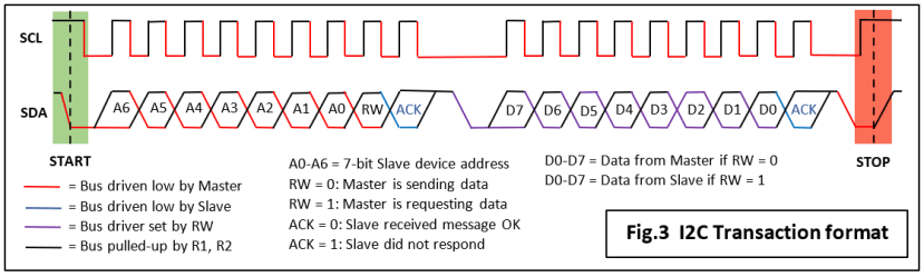
- It allows bi-directional communication along the single data line SDA.
- The Slave can indicate a successful transaction by pulling down SDA during the Acknowledge (ACK) bit interval. If the Master reads a high level (NACK) on SDA at this time it can deduce Slave failure (Fig.3).
- The Slave can signal the Master that it’s not ready by pulling down the clock signal SCL. This useful feature is called ‘clock stretching’ and is supported by many devices on the market.
The I2C two-wire arrangement is very much a minimum hardware-overhead solution, but it has its limitations:
- Only Half-Duplex communication is possible; no simultaneous data movement in both directions.
- The passive pull-up limits the maximum clock frequency and hence the data rate. A Slave’s clock speed is set by the device manufacturer to one of four ‘standard’ values: 100kbit/s, 400kbit/s, 1Mbit/s or 3.4Mbit/s. Some chips can manage 5Mbit/s, but only with push-pull drivers and a unidirectional bus.
- A multi-slave design with no hardware device selection results in a more complex communications protocol with message bytes given over to carrying device addresses.
Ideal for Embedding
If your project requires no GPIO then the low pin-count I2C peripheral chips can be matched to an equally tiny MCU package. The Microchip PIC12F1840 is an excellent example – it only has eight pins, two of which can be set up as an I2C bus.
The Protocol
Philips did a really good job of the I2C bus: they produced a very robust, tightly specified design. The hardware interface is pretty complicated, but the designer need not concern themselves with that because practically every microcontroller currently available has it built-in. The same is true of many slave peripheral devices. The diagram in Fig.3 illustrates the basic components of a Message formed from two or more 9-bit Transactions beginning with a Start sequence and ending with a Stop sequence. The Master MCU does most of the ‘talking’ – the parts in Red and, if sending data to the Slave, i.e. when RW = 0, the parts in Purple. The Slave responds with ACK = 0, the parts in Blue, if a transaction has been received successfully. If RW = 1 then the Slave takes control of SDA and sends the parts in Purple back to the Master. These coloured lines indicate which end is actively pulling down the bus signals; Black lines show the passive pull-up action of the resistors R1 and R2.
Start and Stop
Unlike a UART-type protocol, the Start and Stop signals are not ‘bits’ added to each end of a transaction. For I2C they define the complete message and consist of the relative sequencing of signal edges on both the SCL and SDA lines:
- Start: SDA driven low followed by SCL driven low.
- Stop: SCL pulled-up followed by SDA pulled-up.
This assumes that both signals are in their ‘idle’ state between messages: that is, pulled-up to a high state by the resistors.
Acknowledge
The ACK bit is not used to indicate errors in the received data. All it really does is tell the Master that the addressed Slave is present and able to respond.
Device Addressing
Commercial I2C Slave chips usually come with a pre-programmed 7-bit device address. Normally the bottom one, two or three bits of the address are brought out to pins on the outside so that jumper-links may be added to differentiate between devices of the same type sharing the same bus lines. For example, the base address might be 40h. If the lowest two bits are determined by the external links to VDD and Gnd, then up to four devices may share the bus on addresses 40, 41, 42 and 43h.
Driver software
Driver software reflects the complexity of the hardware, but fortunately MCU manufacturers usually supply development systems with code libraries. I can’t provide a basic ‘snippet’ of code as I did for the UART and SPI articles, but if you’re interested check out the I2C section in the source for FORTHdsPIC. Most of the ‘low-level’ stuff is written in dsPIC33 assembler code.
For an external I2C tutorial with a lot more detail than I can manage here, click on this link.
Finally
A few years after Philips released I2C, Motorola introduced the SPI bus. It was much simpler both in hardware and software and a whole lot faster. The end user often has to create custom drivers for a particular application and it’s less robust. But it is fast. Which is why memory devices with a serial interface, such as Flash and SRAM, will usually use SPI.
In my next missive I’ll describe the robot end of my wireless remote-control project, featuring the I2C-based SRF08 range finder (heading photo). I'll also go through some of the common mistakes made when designing an I2C bus link. And how to fix them.
Previous content in this series
Serial Peripheral Interface (SPI)
Prototyping a wireless robot control box
If you're stuck for something to do, follow my posts on Twitter. I link to interesting articles on new electronics and related technologies, retweeting posts I spot about robots, space exploration and other issues