What is PNP Transistor & its Types
Follow article
 Dave from DesignSpark
How do you feel about this article? Help us to provide better content for you.
Dave from DesignSpark
Thank you! Your feedback has been received.
Dave from DesignSpark
There was a problem submitting your feedback, please try again later.
Dave from DesignSpark
What do you think of this article?
Definition:
The PNP transistor is a type of transistor in which one n-type material is doped with two p-type materials. It is a device that is controlled by the current. Both the emitter and collector currents were controlled by the small amount of base current. Two crystal diodes are connected back-to-back in the PNP transistor. The emitter-base diode is located on the left side of the diode, while the collector-base diode is located on the right side.
The current in the hole is made up of the majority of carriers of the PNP transistors. The current inside the transistor is created by the movement of holes, and the current in the transistor's leads is created by the flow of electrons. When a small current flow through the base of the PNP transistor, it turns on. The current in a PNP transistor flows from the emitter to the collector.
The voltage required by the transistor's emitter, collector and base is indicated by the letter of the PNP transistor. In comparison to the emitter and collector, the base of a PNP transistor has always been negative. The electrons in a PNP transistor are taken from the base terminal. The current that enters the base is amplified before it reaches the collector ends.
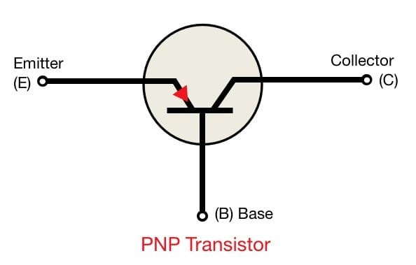
Symbol of PNP Transistor:
The PNP Transistor is denoted by the letters PNP. In the diagram below, the symbol for a PNP transistor is depicted. In a PNP transistor, the current flows from the emitter to the collector, as shown by the inward arrow.
Construction of PNP Transistor:
The structure of a PNP transistor is depicted in the diagram below. The emitter and base junctions are forward biased, while the collector and base junctions are reverse biased. The forward biased emitter attracts electrons to the battery, causing current to flow from the emitter to the collector.
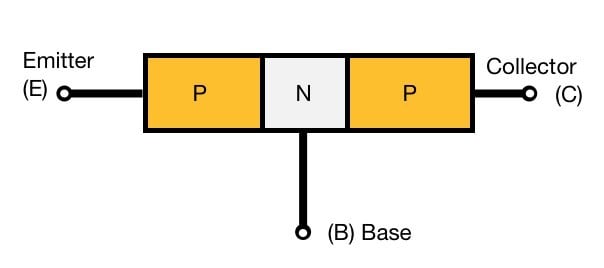
Doped semiconductors are found in three sections of a transistor. On one side, there is an emitter, and on the other, there is a collector. The base refers to the area in the middle. The transistor's three components are described in detail below.
Emitter:
The emitter's job is to provide charge carriers to the receiver. When compared to the base, the emitter is always forward biased in order to supply a large number of charge carriers.
Base:
The base of a transistor is the section in the middle that forms the two PN-junctions between the emitter and the collector. The base-emitter junction is forward biased, allowing the emitter circuit to have low resistance. Due to the reverse bias of the base-collector junction, the collector circuit has a high resistance.
Collector:
The collector is the section on the opposite side of the emitter that collects the charges. When it comes to collecting, the collector is always biased in the opposite direction.
The transistor is equivalent to two diodes because it has two PN-junctions. Emitter-base diode or emitter diode is the name for the junction between the emitter and the base. The junction between the collector and the base is referred to as a collector-base diode or a collector diode.
Working of PNP Transistor:
Because the emitter and base junctions are forward biased, the emitter pushes the holes in the base region. The emitter current is made up of these holes. These electrons combined with the electrons when they moved into the N-type semiconductor material or base. The transistor's base is thin and does not have much doping. As a result, only a few holes combine with electrons, and the rest of the holes are moved to the collector space charge layer. As a result, the base current develops.
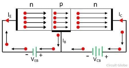
Reverse bias is used to connect the collector-base region. The collector collects or attracts the holes that collect around the depletion region when they were exposed to negative polarity. The collector current develops as a result of this. The collector current IC allows the entire emitter current to pass through.
Curves & Operating Modes of Transistors:
The modes of operation, when used for switching applications, can be divided into four categories based on the biassing of the internal diodes of a transistor. Cut-off, active, saturation, and breakdown regions are the different modes of operation.
Active mode:
The transistor is frequently used as a current amplifier when in this mode of operation. The transistor's two diodes are biased in opposite directions, meaning one is forward biased and the other is reverse biased. Current flows from the emitter to the collector in this mode.
Cutoff Mode:
Both diodes in the transistor are reverse biased when in this mode of operation. The transistor is said to be in the OFF state because no current flows in any direction in this mode.
Saturation mode:
Both diodes in the transistors are forward biased in this mode of operation. Current flows freely from the collector to the emitter in this mode. When the voltage across the base-emitter junction is high, this happens. The ON state is referred to as this mode.
Breakdown Mode:
When the collector voltage exceeds the set limits, the collector diode is destroyed, and the collector current skyrockets to dangerous levels. As a result, a transistor in the breakdown region should not be operated. For example, in a 2N3904 transistor, if the collector voltage exceeds 40V, the breakdown region begins immediately, causing the transistor circuit to be damaged.
Applications:
- Amplification circuits make use of them.
- In Embedded Projects, transistors are used as a switch, and because of fast switching, they are also used for generating PWM signals.
- Darlington (multi-transistor configuration) pair circuits use them.
- In electric motors, PNP transistors are used to control current flow.
- In matched pair circuits, PNP transistors are used to generate contentious and simultaneous power.
The Benefits of a PNP Transistor:
The following are some of the benefits of PNP Transistors:
- To source current, PNP Transistors are used.
- Because it generates a signal that is referenced to the negative power supply rail, it simplifies the circuit design.
- In comparison to NPN Transistors, they produce less noise.
- It's smaller than other transistors and can be used in Integrated Circuits, just like the others.