Debug SPI communication protocol with Analog Discovery 2
Follow article Dave from DesignSpark
How do you feel about this article? Help us to provide better content for you.
Dave from DesignSpark
Thank you! Your feedback has been received.
Dave from DesignSpark
There was a problem submitting your feedback, please try again later.
Dave from DesignSpark
What do you think of this article?

SPI Communication
The Serial Peripheral Interface (SPI) is a duplex synchronous serial communication interface specification used for short-distance communication, primarily in embedded systems. It is commonly used for communication with flash memory, sensors, real-time clocks (RTCs), analog-to-digital converters, and more. SPI can also support having multiple slave devices, but additional slave select (SS) signal would need to be added. You can explore how SPI works at Digilent learn materials.
SPI communication protocol uses four communication pins along with a power and ground pin. There is generally a “master” device and a “slave” device that communicate with one another. The “master” will select one of its “slaves” with its slave select (SS) communication line to indicate to the "slave" that it is going to communicate with it. The master and the slave will then simultaneously communicate with each other on the MOSI (Master Out Slave In) and the MISO (Master In Slave Out) data lines. Both the master and slave send one bit to each other before the actual data are sent to make sure the SPI works. The data can either be sent from the most significant bit (MSB) or the least significant bit (LSB).
To initiate the communication, the master device must bring the chip select (CS) line to a low voltage state and maintain that low voltage state throughout the entire communication session. Both the master and the slave devices will send a bit to each other to make the SPI communication works. Data can then be simultaneously transferred one bit at a time between the two devices. The microcontroller platform controls the timing of the data transfer.
Commonly, the SPI protocol transfers one bit of data on the falling edge of the serial clock (SCK) signal. The data must be put on the data line before the falling edge of the serial clock (SCK). The serial clock (SCK) line must also be at a high voltage state prior to "falling" to a low voltage state (i.e. before falling edge). This can be done with a microcontroller by changing the voltage state of the data line prior to bringing the clock signal to a low voltage state.
The cycle of changing the bit value (voltage) on the data line and pulsing the serial clock (SCK) line will continue until all required bits are transferred. The chip select (CS) line will be brought to a high voltage state. Then, the microcontroller knows that communication has been completed and prepares for another session.
A timing diagram of SPI communication is provided below.

SPI time diagram from Digilent learn materials
Debug SPI Communication
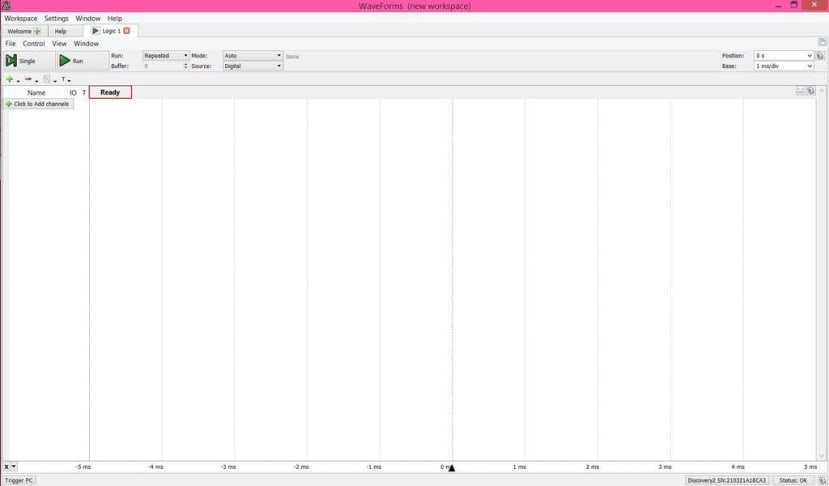
Digilent Analog Discovery 2 (134-6480) is a multi-function instrument which you can measure, visualize, generate, record, and control mixed-signal circuits of all kinds. There are 16 channels for digital inputs or outputs. You can get access to its Logic Analyzer, through Digilent Waveforms, multi-instrument software application to debug the SPI communication.
There is example project to show you how to do so. In the project, you use the Digilent Pmod MIC3 (master) and Digilent Basys 3 (slave) to create the SPI communication. After the hardware is set up properly. You can debug the SPI communication with Analog Discovery 2.

For example, you can create individual signals including CS, SCK, MOSI, MISO and SCK and SPI protocol in the Logic Analyzer at the same time to look at each signal in the communication.

Add SPI protocol
Add Digital Signal
You can use the Logic Analyzer in Waveforms to visualize the SPI communication.

Timing Diagram in Logic Analyzer
The step by step tutorial for this project is available on the Digilent Project Page.