It’s A Small World, After All
Follow article
 Dave from DesignSpark
How do you feel about this article? Help us to provide better content for you.
Dave from DesignSpark
Thank you! Your feedback has been received.
Dave from DesignSpark
There was a problem submitting your feedback, please try again later.
Dave from DesignSpark
What do you think of this article?
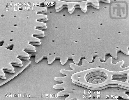
Courtesy Sandia National Laboratories, SUMMiT™ Technologies, www.sandia.gov/mstc
Sometimes you just need someone to ask the right (and in hindsight, obvious) question. But for something good to happen, that question needs to be asked at the right time: when the groundswell of technological development is at a point to begin addressing the question.
A ‘Little’ History
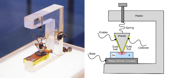
A few months after the December 23rd, 1947 demonstration at Bell labs of the (delightfully home-made looking) PNP point contact germanium transistor, the team lead William Shockley invented a much more robust ‘sandwich structure’ transistor that went on to evolve into the bipolar junction transistor that became ubiquitous from the 1950's onward.
Courtesy Bell Labs
In 1954 Charles S Smith discovered that the resistance of a germanium or silicon filament changed when the material was stressed. The piezoresistance effect is similar to the strain gauge effect seen in metals but, crucially, can be two orders of magnitude greater: making its applicability to sensors obvious from the outset. Silicon strain gauges were being developed commercially by 1958.
Also in 1958, Jack Kilby had just joined Texas Instruments and hadn’t accumulated any vacation time, so when the rest of the company left for their traditional two week vacation, he was left alone in the lab to test some of his ideas.
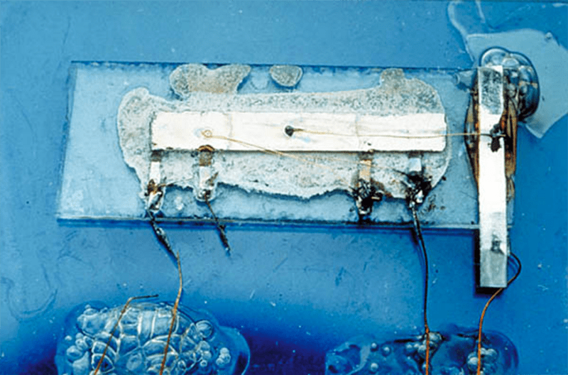
On a germanium slab 7/16th by 1/16th of an inch, he built a circuit with 1 transistor, 3 resistors and a capacitor, which he demonstrated producing a continuous sine wave on September 12th of 1958.
Robert Noyce (who went on to co-found Fairchild Semiconductor and Intel) had been working on the same concept in silicon. In March 1961 Fairchild released their first digital logic function IC with four transistors and five resistors. Although not first, the silicon IC ended up fairing much better commercially.
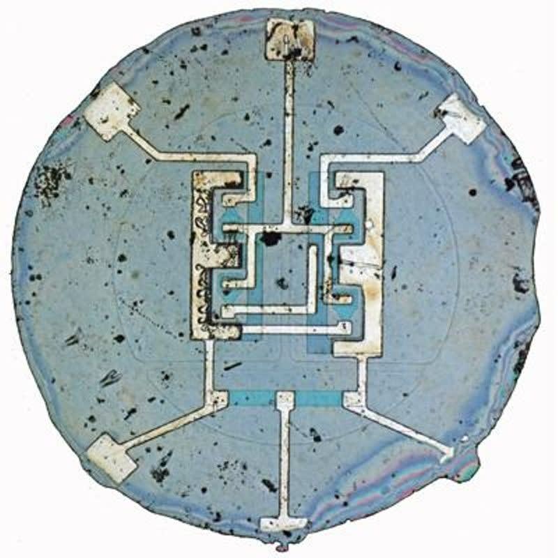
Courtesy Fairchild Semiconductor
So you see, when renowned Physicist Richard Feynman presented “There’s Plenty of Room at the Bottom” to the American Physical Society in 1959, there was already fertile ground for the idea of manipulating matter at the atomic scale to produce micro technology. Many technology historians see this lecture as the start of the MEMS revolution.
MEMS
At this point you may be thinking: “Redstone, you incredibly suave raconteur, what are these MEMS you speak of?” Well, I’m glad you asked.
MicroElectroMechanical Systems – sometimes referred to as ‘Micromachines’ in Japan, or Microsystems Technology (MST) in parts of Europe – is a spin-off technology derived from the microelectronics industry. Fabrication techniques developed to build integrated circuits were modified over time into sophisticated micromachining processes such as bulk and surface micromachining or high aspect ratio micromachining (HARM). These techniques selectively remove areas of silicon or add extra structural layers to form complex mechanical or electromechanical components which exploit both the electrical and mechanical properties of silicon.
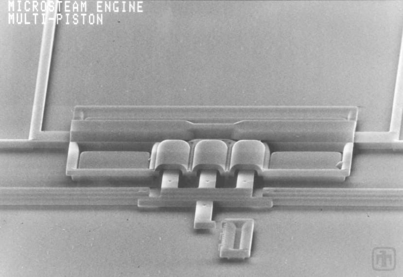
3 Piston Steam engine Courtesy Sandia National Laboratories, SUMMiT™ Technologies, www.sandia.gov/mstc
The resulting components or devices range in size from as small as 1µm up to around 1mm. Levers, fluid channels, gears, pistons, motors – even steam engines have all been fabricated using these techniques. It is perhaps worth pointing out that the ‘micro’ in MEMS refers to these micromachined components, not the entire system, which will also tend to include integrated electronics for supplying power, controlling the device and external communications.
Why So Small?
“But Redstone, you delightful opiate of the masses,” I hear you say; “aren’t most of these devices used in large machinery? Why make them so small?” Another good question. You’re really paying attention today. The answer lies in taking advantage of scaling laws.
Generally speaking, smaller things are less affected by volume dependent phenomena like mass (and its inherent inertia) but more affected by surface area phenomena like heat transfer or contact force.
To help explain what we mean, consider a simple cube where each side has a length of ‘a’:

What does this mean? Well, as the volume (which is proportional to the heat storage ability) of a shape decreases, the surface area (which is proportional to the heat dissipation) proportionally increases. So, the same shape becomes proportionally better at dissipating heat, the smaller it gets.
As another example, we also find that the spring constant of a beam decreases proportionally with the beam size; which means that the smaller a beam gets, the more flexible it is.
When we take advantage of these kinds of scaling factors we find that micro-scale sensors have higher sensitivity, better linearity, better response times and dynamic range than their full-scale cousins. Micro-scale actuators have better dynamic response speeds and much lower power consumption. Both device types benefit from the manufacturing cost reductions afforded by batch fabrication.
Into The Real World
The making of the current MEMS industry was the automotive airbag. The MEMS accelerometers that began replacing the conventional mechanical ball and tube devices in the early 1990’s were one of the first commercial applications of this technology.
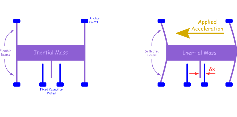
The accelerometer is a capacitive (or piezoresistive) device made up of a suspended pendulum proof mass and plate assembly. As acceleration acts on the proof mass, the capacitance between the plates changes. This change is detected and processed so that the system can act accordingly.
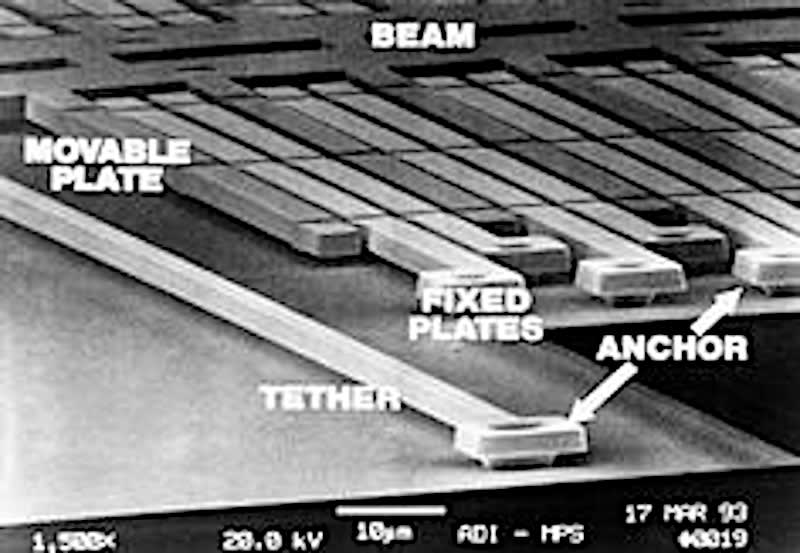
ADXL50 Accelerometer Courtesy Analog Devices
By the year 2000, around 60 million of these accelerometers were being used in the field. Reliably operating in the challenging range of environments found in vehicles, silenced sceptics and prompted the explosion of their use in other automotive applications such as active suspension systems, anti-lock braking, appliance and navigation controls, fuel sensors, noise reduction, rollover detection, seatbelt restraint and tensioning, vibration monitoring etc.
Away from the automotive industry, Apple’s iPhone 4 was revolutionary in being the first portable consumer device to be set up to sense motion through a full 9 degrees of Freedom (DoF). This was done by incorporating a 3-axis accelerometer, a 3-axis gyroscope and 3-axis electronic compass.
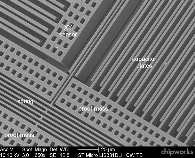
If you had ripped the back off your iPhone 4 in a drunken fit of curiosity (what? It happens…), you would have found a couple of ST Micro devices close to the A4 processor; an LIS331DLH accelerometer and a L3G4200D gyroscope, though the devices weren’t labelled with ST Micro part numbers. The Asahi Kasei AKM8975 electronic compass was on the other side of the main board.
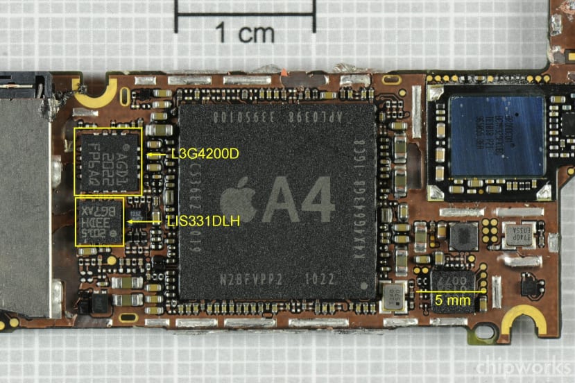
Courtesy Chipworks
The LIS331DLH had two chips inside the package, an ASIC to process the signals from the MEMS structure and our MEMS accelerometer itself. Unlike other vendors, ST Micro had stacked the ASIC over the top of the MEMS device which allowed for a smaller footprint. The device connected to the A4 processor with a standard I2C/SPI serial interface. Zooming in for a view of the X-Y plane sensor, we can see the exquisite detail that micromachining allows:
Forward into Industry 4.0
"But Redstone, you cheeky disseminator of interesting information," I hear you say, "what's going on with MEMS now?" That’s another good question.
The latest generation of MEMS devices have, in many ways, followed the increased integration of electronic ICs and now often combine multiple functions into a single unit.
Inertial Measurement Units (or IMUs), will usually include at least three axes of accelerometers (measuring acceleration and angular orientation), three axes of gyroscopes (measuring angular velocity) and often also include 3-axis magnetometers, which measure magnetic field intensity.
An accelerometer measures static and dynamic acceleration in the direction of each of its axes. “Static acceleration” sounds odd but is an important sensor behaviour: a response to gravity. With no dynamic acceleration, each accelerometer output will represent the orientation of the axis with respect to gravity.
All vibratory gyroscopes measure angular velocity using the Coriolis acceleration that arises in a rotating reference frame:
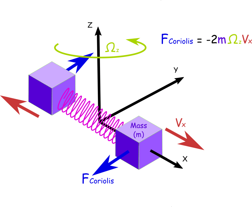
“But Redstone, you font of exquisitely crafted prose,” I hear you say, “You know Coriolis force is supposed to be fictitious, don’t you?” Why yes, yes I do. But here’s the thing – the effects are easy to measure accurately, so let’s just leave it at that and move on.
The 3-axis magnetometer measures magnetic field intensity from three orthogonal axes to estimate orientation angle with respect to the localised direction of the earth’s magnetic field. The magnetometer can improve positioning measurement accuracy in some systems but can be thrown by strong sources of dynamic field disturbance, like electric motors so are not included in all IMUs.
Integrating and calibrating these devices in the same package along with a processing ASIC makes it possible to apply filters and fusion routines (combining readings from multiple sensor types to get a best estimate) to the raw measurements. Some devices even include machine learning cores. This all means that the microcontroller in an IoT or industrial control environment is relieved of the burden of all these calculations and can just make rapid (and low power) decisions based on the digital information it gets over the serial interface.
Modern IMUs can be used as part of a closed-loop control system to actively reduce vibration or compensate for dynamic displacements, like you would find on a moving vehicle. The feedback sensor provides dynamic orientation information for the instrument platform and a feedback controller processes this information, translating it into corrective control signals for servo motors. What makes IMUs exciting in industry is their ability to linearly handle vibration frequencies from 5 Hz to 500 Hz with accelerations as high as 25 g.
To put that into perspective, an average person (untrained in the G-straining manoeuvre) can black out as low as 6 g (and that is without oscillating at 5 to 500Hz) while the highest g-force which can be experienced on a roller coaster today is 6.3 g on ‘Tower of Terror’ at Gold Reef City in South Africa. Definitely on my bucket list!
Getting Involved
As we have already hinted at, the breadth of MEMS devices is huge, encompassing pretty much any kind of transducers or actuator you can think of. To name just a few:
- Inkjet printer heads: use piezoelectrics or thermal bubble ejection through micromachined fluid channels.
- Digital Micromirror Devices: DMDs use hundreds of thousands of individually adjustable micro mirrors to create razor sharp projected images.
- Microphones: used in portable devices and Bluetooth headphones.
- Loudspeakers: for in-ear headphones or hearing aids
- Optical switching technology: used for both switching and alignment in optical data communications technology.
- Pressure sensors: in your vehicle tyres or even in arteries for disposable blood pressure monitors.
- Microscale energy harvesting: uses piezoelectric, electrostatic and electromagnetic devices to harvest energy making low power systems self sustaining.
The list goes on and it is an ever-expanding field. One of the interesting developments in recent years has been in the field of BioMEMS from embedded medical devices (such as stents) to Lab-On-Chip devices.
We mentioned the ST Micro MEMS devices in the iPhone 4 earlier. If you head over to their current MEMS page you can see that things have moved on since those heady days. There is a broad range of products covering consumer, automotive and industry 4.0 applications.
I guess one group that catches the eye, given all we have had to say on IMUs is the iNEMO™ inertial modules (875-0918) and (875-0927) . These IMUs include an embedded machine learning core that can run an in-sensor classification engine.
If you want to get a jump start on developing with MEMS sensors, you could try out the new STWIN SensorTile wireless industrial node STEVAL-STWINKT1 (193-9794) .